Waveguide Configurations for Minimising Substrate Area

Inactive Publication Date: 2008-05-08
ZETTA RES & DEV LLC RPO SERIES
View PDF32 Cites 48 Cited by
  • Summary
  • Abstract
  • Description
  • Claims
  • Application Information

AI Technical Summary

Benefits of technology

[0024] The term “crossing over” is to be construed as either the passing of one waveguide through another (in other words, the coplanar intersection of waveguides), or alternatively, a configuration whereby one waveguide forms a bridge over another waveguide. Both of these constr

Problems solved by technology

The most common approach uses a flexible resistive overlays although the overlay is easily damaged, can cause glare problems, and tends to dim an underlying screen, requiring excess power usage to compensate for such dimming.
Resistive devices can also be sensitive to humidity, and the cost of the resistive overlay scales quadratically with perimeter.
In this case the overlay is generally more durable, but the glare and dimming problems remain.
They have the advantage of being overlay-free and can function in

Method used


Image

  • Waveguide Configurations for Minimising Substrate Area
  • Waveguide Configurations for Minimising Substrate Area
  • Waveguide Configurations for Minimising Substrate Area

Examples


first embodiment

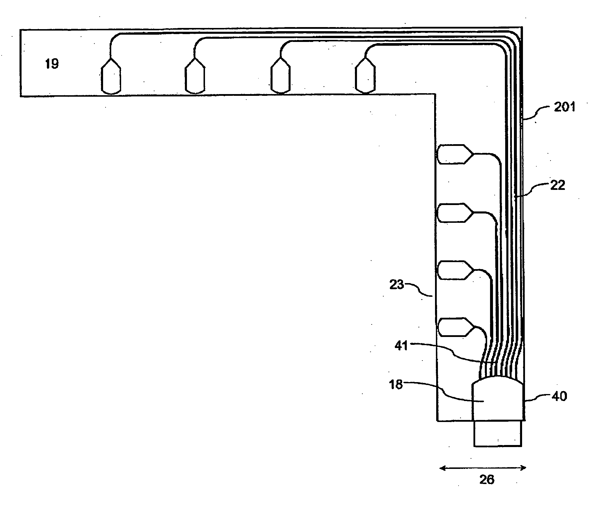
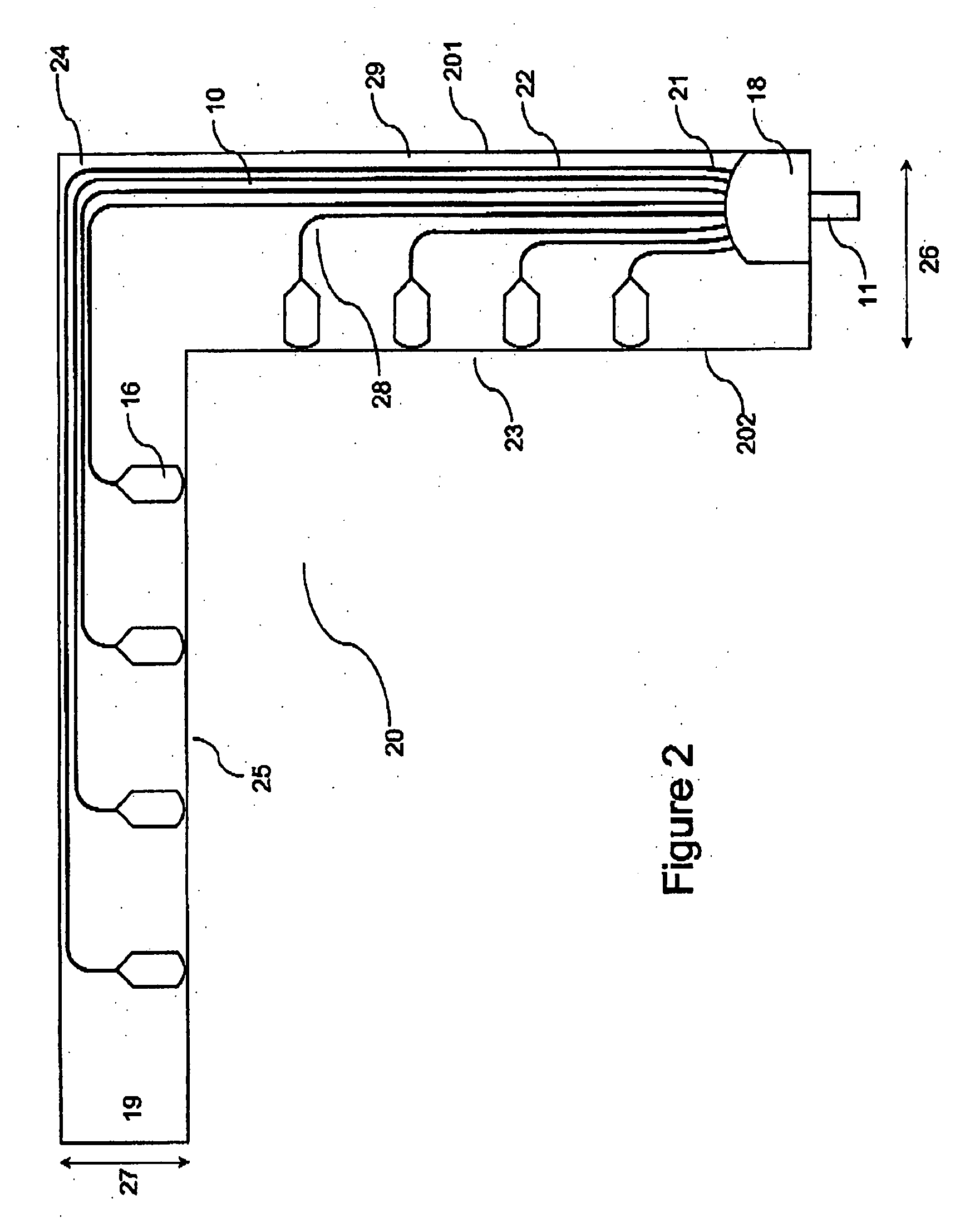
[0052] According to the present invention, illustrated in FIG. 4, the gap 29 can be reduced by offsetting the 1×N tree splitter 18 with respect to the waveguide fairway 22, such that the edge 40 of the splitter's diffractive slab region coincides with the outermost waveguide of the fairway 22. The outer edge 201 of the substrate 19 can then be brought to within the dicing margin of the splitter edge 40 and the fairway 22. This offset is achieved by introducing an S-bend 41 into the waveguides after they emerge from the 1×N tree splitter, and reduces the width 26 of the (wider) first leg 23 of the substrate 19 by 0.8 mm. On the receive side, a similar S-bend could be used to eliminate any ‘dead zone’ between the edge of the multi-element detector and its array of detector pixels.

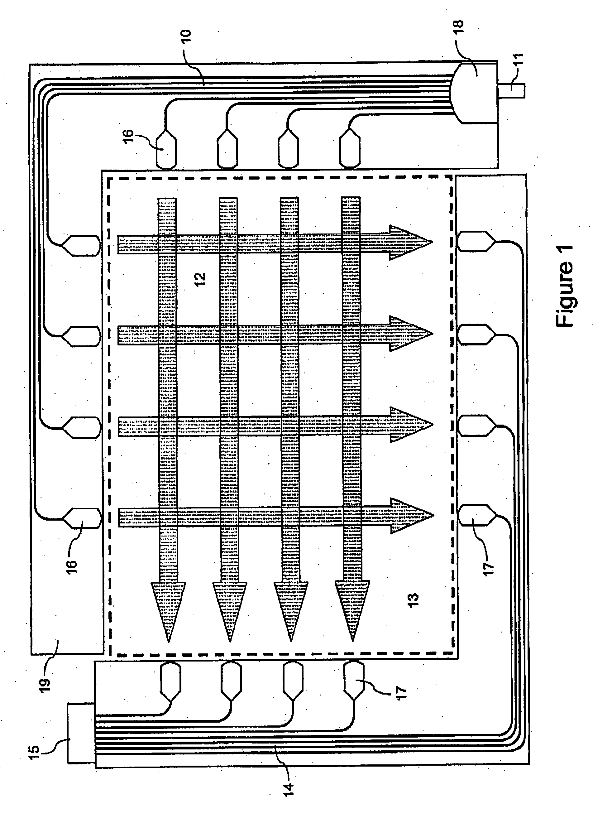
[0053] We now turn to consideration of the contribution to bezel width made by the waveguide bends 28. For right angle bends 28 as shown in FIG. 2, the contribution to bezel width is equal to the bend radius,...

second embodiment

[0054] According to the present invention, the bend-related contribution to bezel width can be reduced by changing the manner in which the waveguides 10 or 14‘peel off’ from their waveguide fairway towards their respective in-plane lenses 16 or 17. Instead of having each transmit waveguide 10 peeling off in turn from the inside of the fairway 22 as shown in FIG. 2, FIG. 5 shows a novel waveguide layout wherein, along at least a first side 23 of the L-shaped substrate 19, each transmit waveguide 10 peels off from the outside of the fairway, thereby crossing all of the remaining waveguides en route to its in-plane lens 16. The ‘inside’ of the waveguide fairway 22 is defined as the side closer to the in-plane lenses 16.

[0055] Unlike the case of an electronic circuit, where such crossings would be forbidden because of electrical shorting, optical waveguides can cross each other with impunity provided the crossing angle θ, as shown in FIG. 6, is sufficiently large. Providing the crossing...

third embodiment

[0057] Nevertheless the ‘outside peel-off’ benefit can be made to apply along the second side 25 by other variations in the waveguide layout. For example FIG. 7 shows a waveguide layout according to the present invention, in which the waveguides 10 in the second fairway 50 gradually bend away from the inner edge 51 towards the outer edge 52 before making the right angle bend 28 towards their respective in-plane lenses 16. With this configuration, the width 27 of the second side 25 is also reduced by an amount equal to the radius of the bends 28, i.e. 1.5 mm, and a similar width reduction would be obtained on the corresponding side of the receive substrate.

[0058] Returning to FIG. 6, we now consider what it means for the crossing angle θ to be ‘large enough’ for there to be negligible crosstalk and scattering loss at a crossing point 60. For crossings involving single-mode waveguides, it is generally accepted that a crossing angle of 20° or more is ‘large enough’, and even if the wav...


PUM


Abstract

The invention describes various optical waveguide layouts with reduced substrate area, with particular application to reducing bezel width in optical touch systems. In certain preferred embodiments the optical waveguide layouts include a plurality of waveguide crossings.

Description

FIELD OF THE INVENTION [0001] The invention relates to the design of an optical waveguide layout for minimising substrate area, and in particular for reducing bezel width in optical touch systems. However it will be appreciated that the invention is not limited to this particular field of use. BACKGROUND OF THE INVENTION [0002] Any discussion of the prior art throughout the specification should in no way be considered as an admission that such prior art is widely known or forms part of the common general knowledge in the field. [0003] Touch input devices or sensors for computers and other consumer electronics devices such as mobile phones, personal digital assistants (PDAs) and hand-held games are highly desirable due to their extreme ease of use. In the past, a variety of approaches have been used to provide touch input devices. The most common approach uses a flexible resistive overlays although the overlay is easily damaged, can cause glare problems, and tends to dim an underlyin...

Claims


Application Information

Patent Timeline
IPC IPC(8): G06F3/042G02B6/32G02B6/10
CPCG02B6/12004G06F3/0421G02B6/125G02B6/1245
Inventor CORNISH, BENJAMINCHARTERS, ROBERT BRUCEHOLLOWAY, WARWICK TODDMAXWELL, IAN ANDREWKUKULJ, DAX
Owner ZETTA RES & DEV LLC RPO SERIES
Why Eureka
Try Eureka