Substrate Processing Apparatus and Method
a substrate and processing apparatus technology, applied in the direction of chemistry apparatus and processes, flexible article cleaning, liquid cleaning, etc., can solve the problems of contamination of substrate, difficult to clean or etch portions of substrate, and complicated structure of conventional substrate processing apparatus, so as to prevent contamination
- Summary
- Abstract
- Description
- Claims
- Application Information
AI Technical Summary
Benefits of technology
Problems solved by technology
Method used
Image
Examples
first embodiment
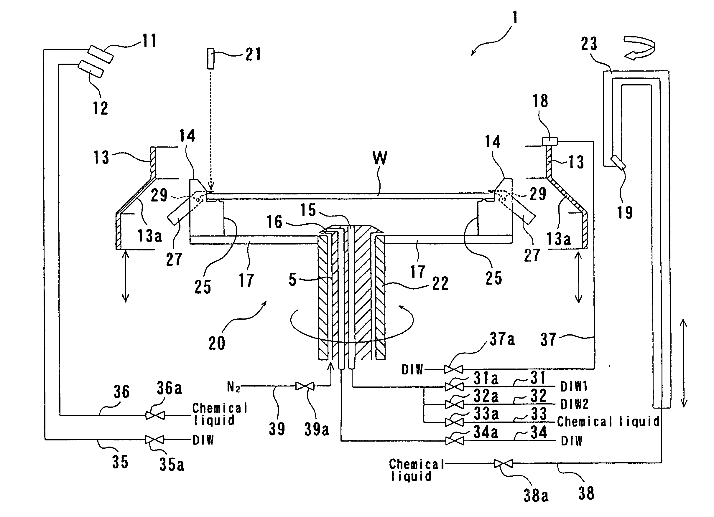
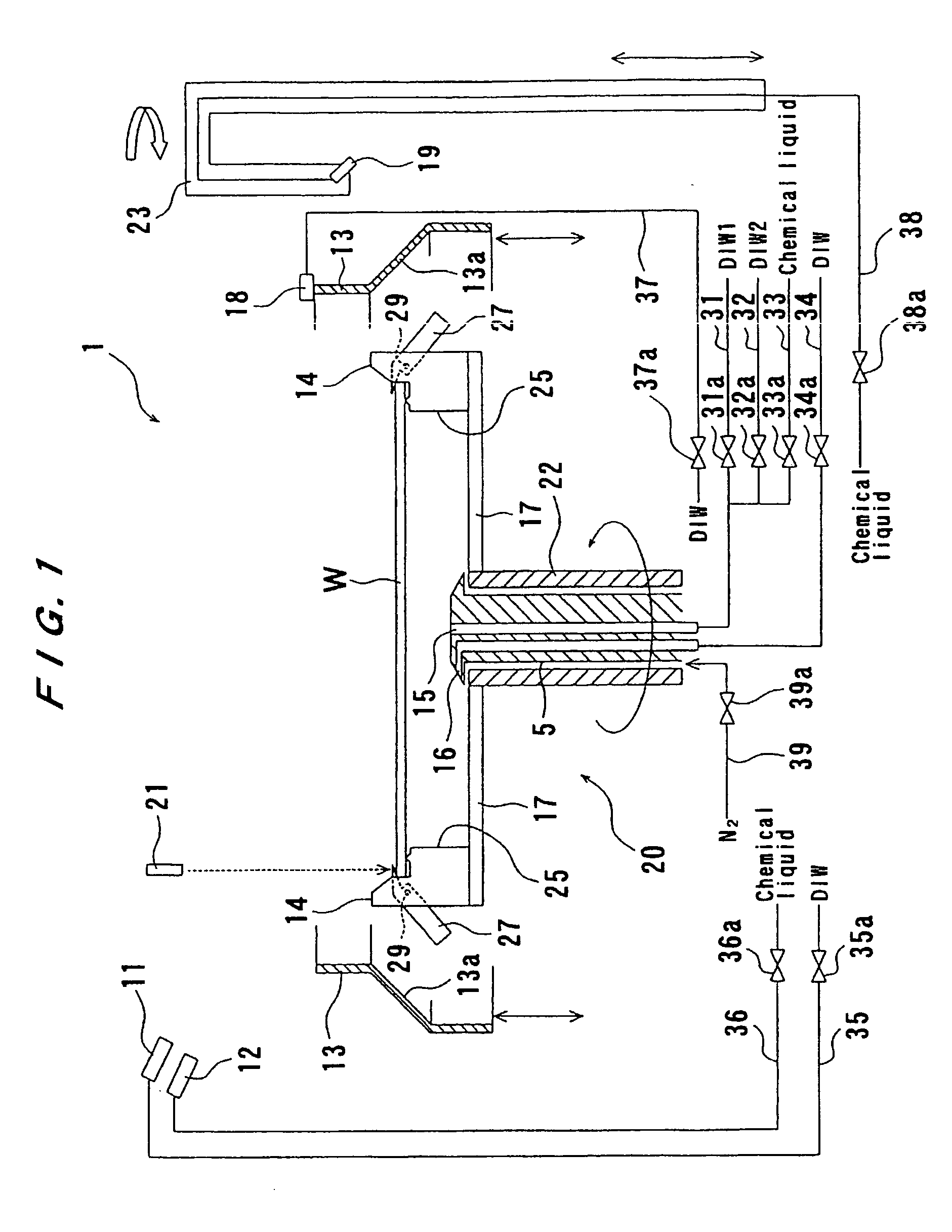
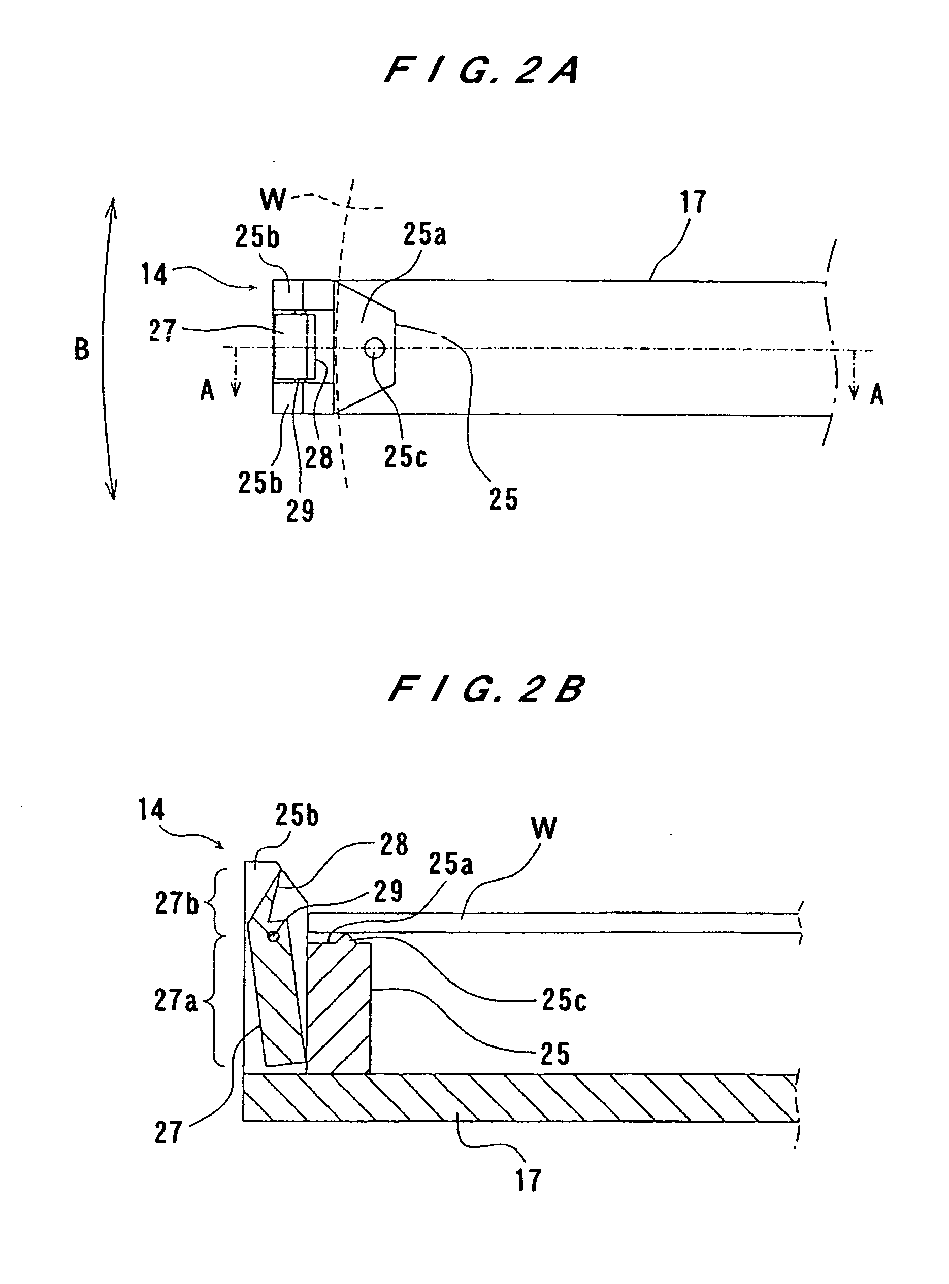
[0056]FIG. 1 shows a schematic arrangement of a substrate processing apparatus 1 according to the present invention. As shown in FIG. 1, the substrate processing apparatus 1 has a substrate holding and rotation mechanism 20 including a rotatable shaft 22 as a substrate rotation mechanism for rotating a substrate W such as a semiconductor wafer to be processed, a plurality of base members 17 extending radially from an upper end of the rotatable shaft 22 in horizontal outward directions, and substrate holding mechanisms 14 provided on tip ends of the base members 17. There are provided a plurality of sets (at least three sets) of the base members 17 and the substrate holding mechanisms 14. The substrate W is held on a central portion of the plurality substrate holding mechanisms 14.
[0057]The substrate processing apparatus 1 has a driving device coupled to the rotatable shaft 22. The substrate holding and rotation mechanism 20 rotates the substrate W about the rotatable shaft 22 while ...
second embodiment
[0110]FIG. 11 is a side view showing a substrate processing apparatus 101 according to the present invention, and FIG. 12 is a plan view showing substrate holding mechanisms (substrate holding chucks) 114 and a base member (chuck holding base) 117 in the substrate processing apparatus 101 shown in FIG. 11. The substrate processing apparatus 101 has a circular base member 117, at least three substrate holding mechanisms 114 (four substrate holding mechanisms in FIG. 12) provided near a peripheral portion of the base member 117 (at positions a predetermined distance inward from a periphery of the base member 117) for holding a substrate W such as a semiconductor wafer, and a rotatable shaft 122 attached to a central portion of the base member 117. The base member 117 is rotated about the rotatable shaft 122 by a driving device (not shown) while the substrate W is held by the substrate holding mechanisms 114. The base member 117 is slightly larger than the substrate W and thus covers t...
PUM
| Property | Measurement | Unit |
|---|---|---|
| Angular velocity | aaaaa | aaaaa |
| Angular velocity | aaaaa | aaaaa |
| Force | aaaaa | aaaaa |
Abstract
Description
Claims
Application Information


