

Protective structure for semiconductor sensors
a technology of protective structure and semiconductor, applied in the direction of measuring devices, instruments, material analysis through electric/magnetic means, etc., can solve the problems of affecting the accuracy of potentiometric measurement, the inability of sensors to detect measured quantities that are exposed to environmental influences in order to be able to protect them from electric or electrostatic overstress as effectively as other semiconductor devices, and the inability to precisely measure the quantity. to achieve the effect of reducing leakage current, ensuring semiconductor process
- Summary
- Abstract
- Description
- Claims
- Application Information
AI Technical Summary
Benefits of technology
Problems solved by technology
Method used
Image

Examples
Embodiment Construction
[0023]Before the present invention will be discussed in the context of the drawings in more detail below, it is pointed out that like elements in the figures are provided with like or similar reference numbers and that a repeated description of these elements is omitted.
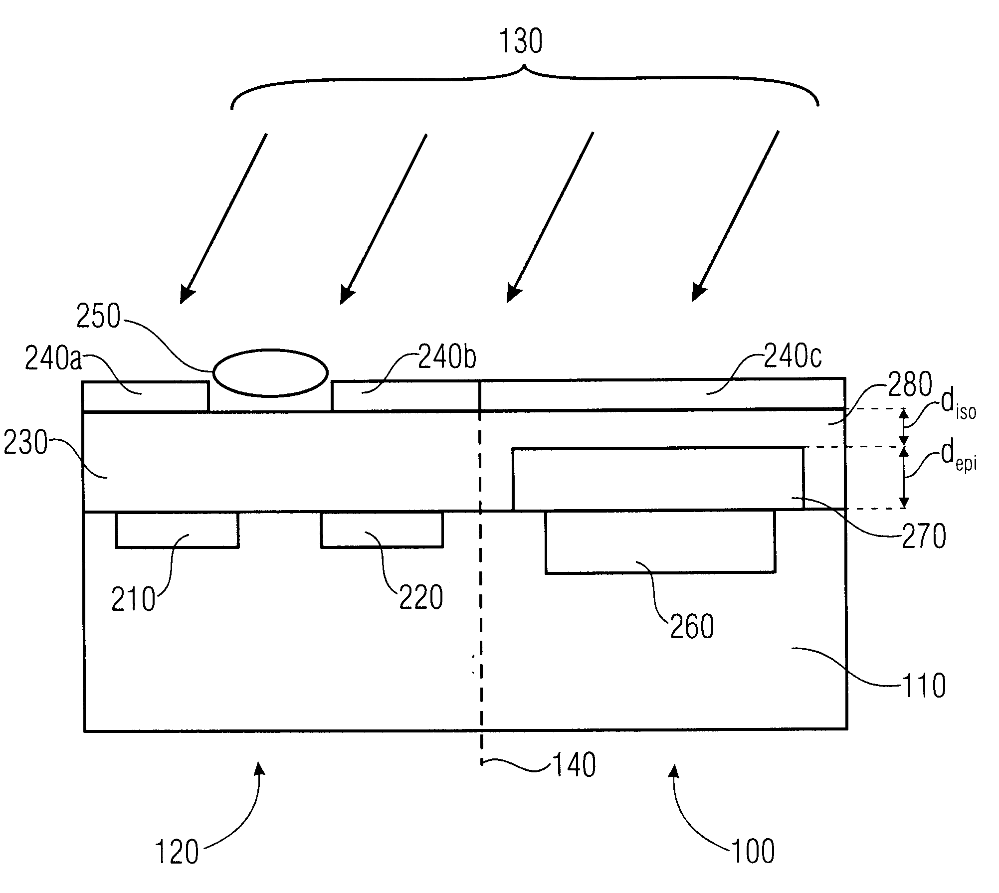
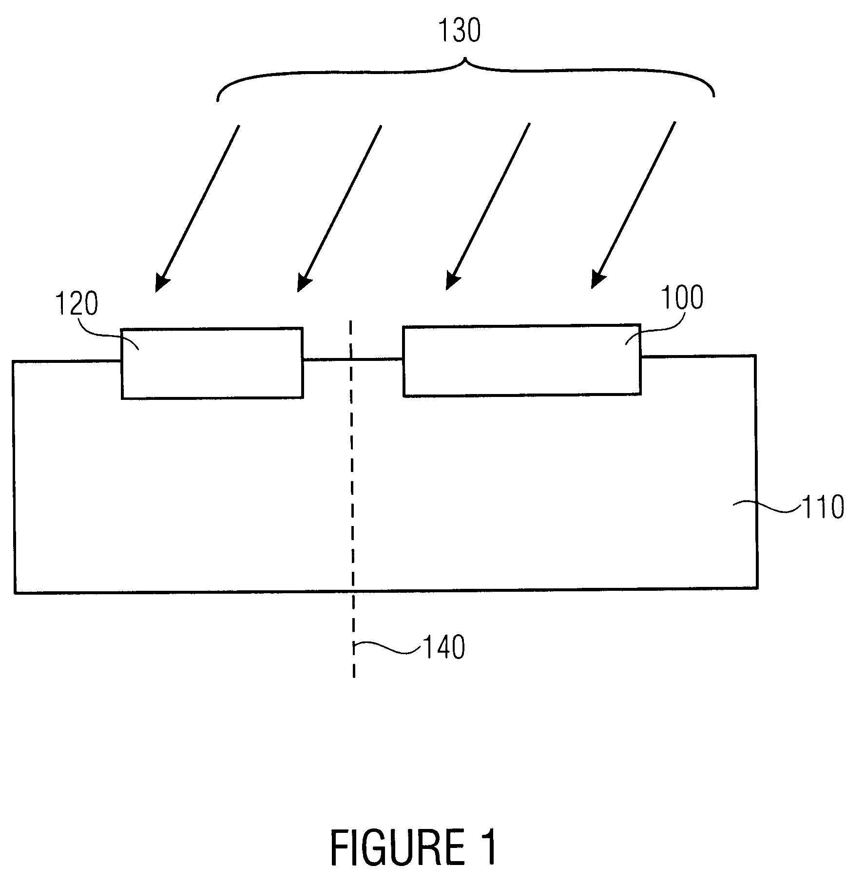
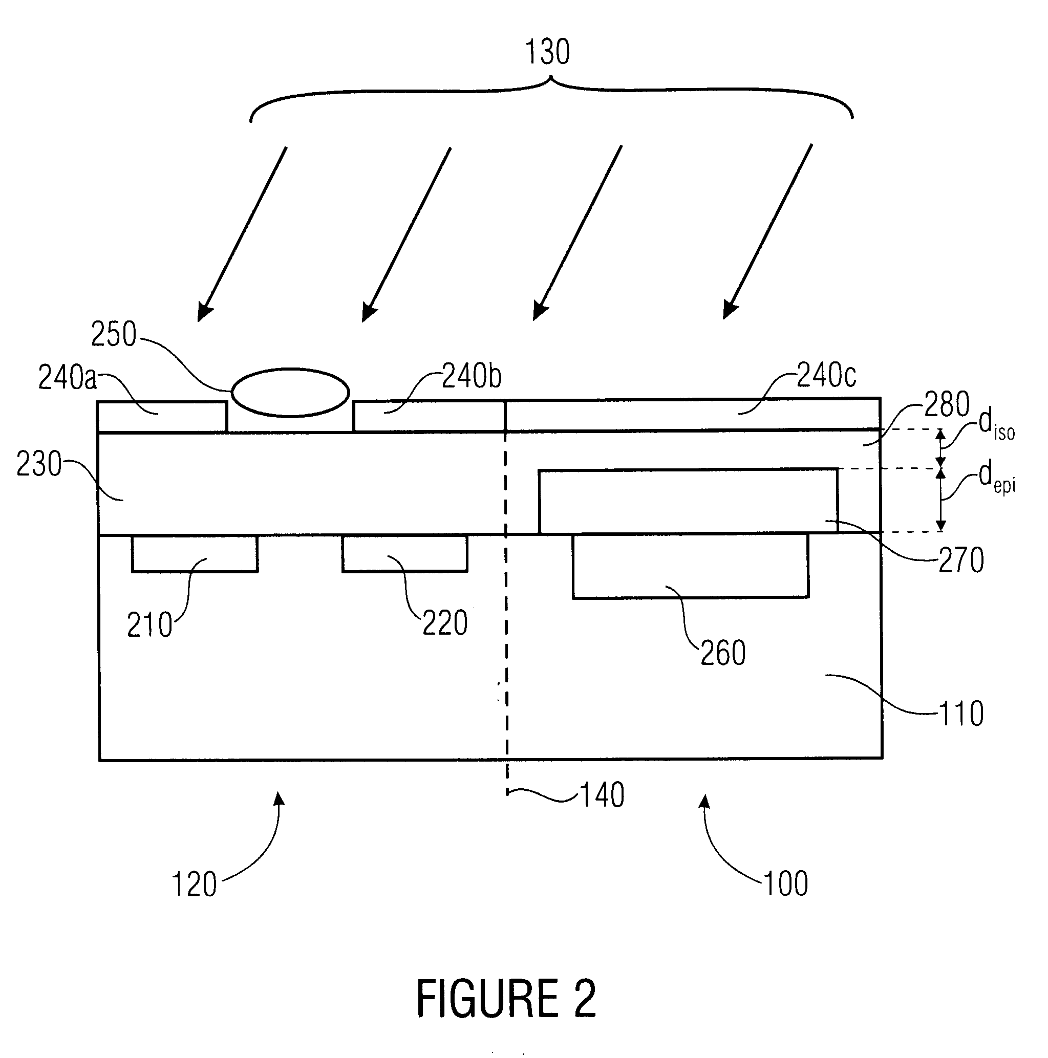
[0024]FIG. 1 shows a schematic representation of a protective structure 100 that is integrated on a substrate 110 along with a semiconductor sensor 120. The protective structure 100 as well as the semiconductor sensor 120 are exposed to a measuring medium 130. According to the invention, the protective structure 100 as well as the semiconductor sensor 120 are thus monolithically integrated in the substrate 110, wherein they are integrated, for example, in different regions of the substrate 110, which are separated in FIG. 1 by a dividing line 140. The dividing line 140 only serves as an illustration of a lateral integration of the protective structure 100 (next to the semiconductor sensor 120) on the same substrate 1...
PUM
 Abstract
Description
Claims
Application Information