
Membrane probing system

a probe and membrane technology, applied in the field of probe assemblies, can solve the problems of excessive pad damage, large signal distortion, and more forward tips of the tip to bear down too heavily on their respective pads

Inactive Publication Date: 2008-05-15
FORMFACTOR BEAVERTON INC
View PDF64 Cites 18 Cited by
  • Summary
  • Abstract
  • Description
  • Claims
  • Application Information

AI Technical Summary

Benefits of technology

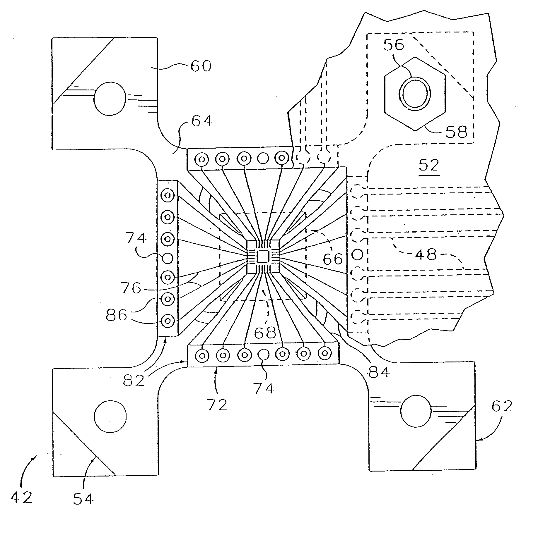
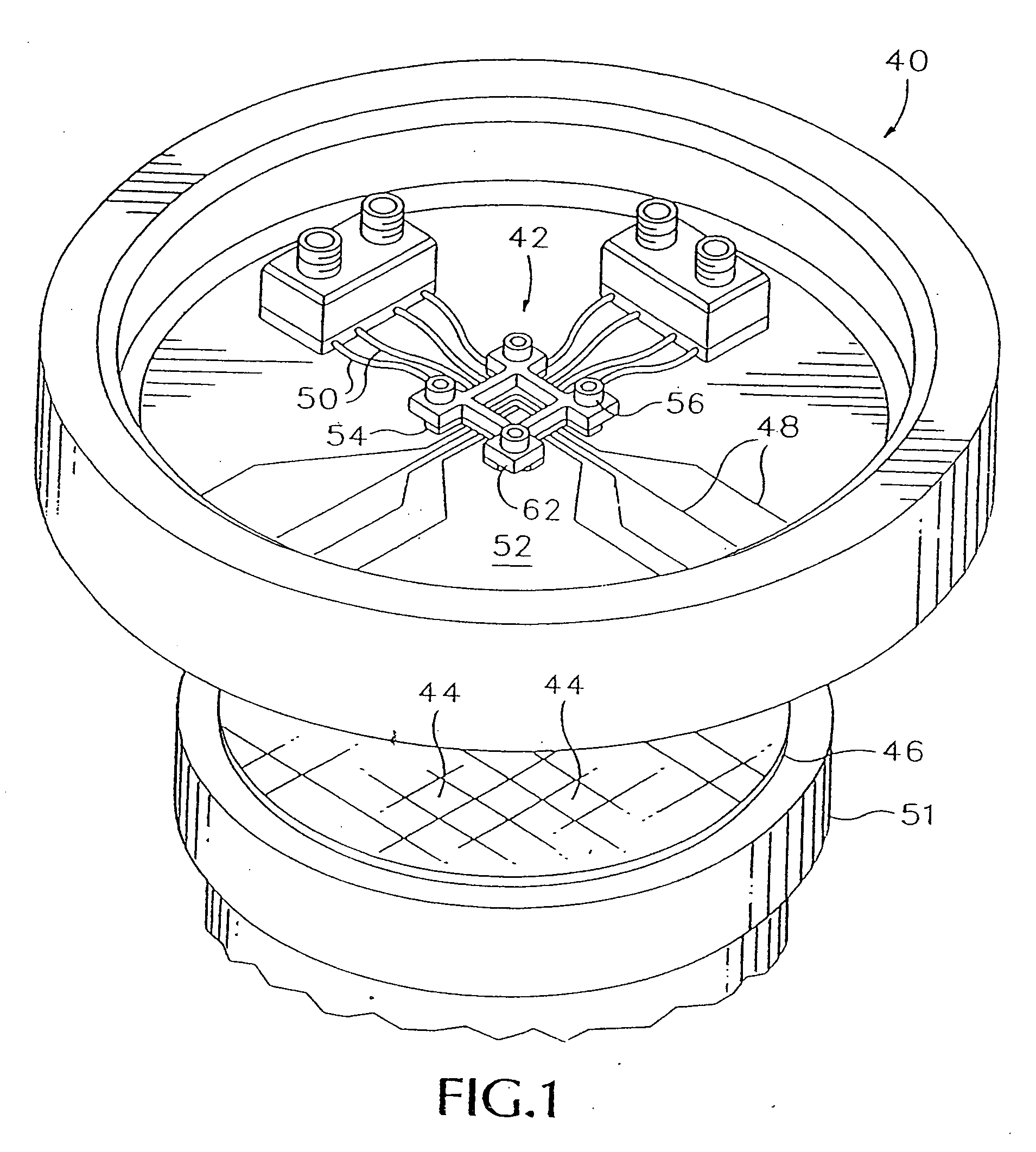
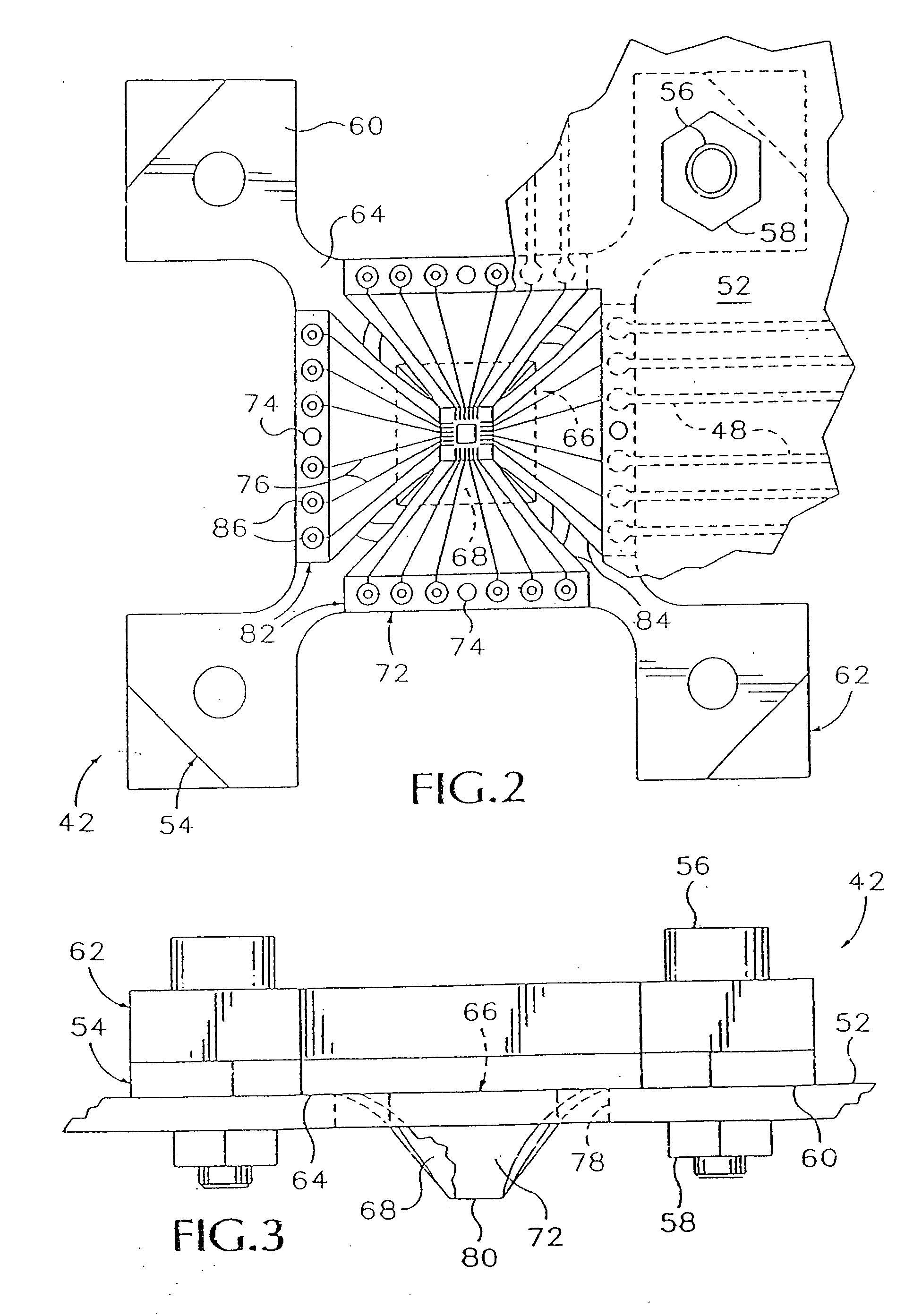
"The present invention is a membrane probing assembly with a probe card that includes conductors supported thereon. The conductors include at least a signal conductor located between a pair of spaced apart guard conductors. A membrane assembly includes a membrane with contacts thereon, and supporting at least a signal conductor located between a pair of spaced apart guard conductors. The guard conductors of the probe card are electrically interconnected proximate the interconnection between the probe card and the membrane assembly. The guard conductors of the membrane assembly are electrically interconnected proximate the interconnection between the probe card and the membrane assembly. This invention solves the problem of prior art where the signal conductor was not protected by guard conductors, which could cause damage to the signal conductor during use. The invention provides a solution by including a probe card with conductors that have guard conductors to protect the signal conductor."

Problems solved by technology

The problem with this type of probing assembly is that the needle-like tips, due to their narrow geometry, exhibit high inductance so that signal distortion is large in high frequency measurements made through these tips.
Also, these tips can act in the manner of a planing tool as they wipe across their respective pads, thereby leading to excessive pad damage.
This problem is magnified to the extent that the probe tips bend out of shape during use or otherwise fail to terminate in a common plane which causes the more forward ones of the tips to bear down too heavily on their respective pads.
Also, it is impractical to mount these tips at less than 100 micron center-to-center spacing or in a multi-row grid-like pattern so as to accommodate the pad arrangement of more modern, higher density dies.
Also, this type of probing assembly has a scrub length of the needle tips of 25 microns or more, which increases the difficulty of staying within the allowed probing area.
However, although several different forms of this probing assembly have been proposed, difficulties have been encountered in connection with this type of assembly in reducing pad wear and in achieving reliable clearing of the oxide layer from each of the device pads so as to ensure adequate electrical connection between the assembly and the device-under-test.
In respect to both of these devices, however; because of manufacturing tolerances; certain of the contact bumps are likely to be in a recessed position relative to their neighbors and these recessed bumps will not have a satisfactory opportunity to engage their pads since they will be drawn away from their pads by the action of their neighbors on the rigid support.
Furthermore, even when “scrub” movement is provided in the manner of Huff, the contacts will tend to frictionally cling to the device as they perform the scrubbing movement, that is, there will be a tendency for the pads of the device to move in unison with the contacts so as to negate the effect of the contact movement.
Hence this form of membrane probing assembly does not ensure reliable electrical connection between each contact and pad.
These alternative devices, however, do not afford sufficient pressure between the probing contacts and the device pads to reliably penetrate the oxides that form on the pad surfaces.
Pad damage is likely to occur with this type of design, however, because a certain amount of tilt is typically present between the contacts and the device, and those contacts angled closest to the device will ordinarily develop much higher contact pressures than those which are angled away.
The same problem arises with the related assembly shown in European Patent Pub.
However, the Evans device is subject to the friction clinging problem already described insofar as the pads of the device are likely to cling to the contacts as the support pivots and causes the contacts to shift laterally.
In both Crumly and Barsotti, however, if any tilt is present between the contacts and the device at the time of engagement, this tilt will cause the contacts angled closest to the device to scrub further than those angled further away.
A further disadvantage of the Crumly device, in particular, is that the contacts nearer to the center of the membrane will scrub less than those nearer to the periphery so that scrub effectiveness will vary with contact position.
It is difficult, however, to originally position these fingers so that they all terminate in a common plane, particularly if a high density pattern is required.
Moreover, these fingers are easily bent out of position during use and cannot easily be rebent back to their original position.
Nor, in Evans at least, is there an adequate mechanism for tolerating a minor degree of tilt between the fingers and pads.
Although Evans suggests roughening the surface of each finger to improve the quality of electrical connection, this roughening can cause undue abrasion and damage to the pad surfaces.
Yet a further disadvantage of the contact fingers shown in both Evans and Higgins is that such fingers are subject to fatigue and failure after a relatively low number of “touchdowns” or duty cycles due to repeated bending and stressing.

Method used


Image

  • Membrane probing system
  • Membrane probing system
  • Membrane probing system

Examples


Embodiment Construction

[0055] With particular regard to probe cards that are specially adapted for use in measuring ultra-low currents, probe card designers have been concerned with developing techniques for controlling (e.g., minimizing) leakage currents. Unwanted currents that flow into a particular cable (or conductor) from surrounding cables (or conductors) may distort the current measured in that particular cable (or conductor). For a given potential difference between two spaced apart conductors, the amount of leakage current that will flow between them will vary depending upon the volume resistivity of the insulating material that separates the conductors. In other words, if a relatively lower-resistance insulator is used, this will result in a relatively higher leakage current. Thus, a designer of low-current probe cards will normally avoid the use of rubber-insulated single-core wires on a glass-epoxy board since rubber and glass-epoxy materials are known to be relatively low-resistance insulator...


PUM


Abstract

A membrane probing assembly includes a probe card with conductors supported thereon, wherein the conductors include at least a signal conductor located between a pair of spaced apart guard conductors. A membrane assembly includes a membrane with contacts thereon, and supporting at least a signal conductor located between a pair of spaced apart guard conductors. The guard conductors of the probe card are electrically interconnected proximate the interconnection between the probe card and the membrane assembly. The guard conductors of the membrane assembly are electrically interconnected proximate the interconnection between the probe card and the membrane assembly.

Description

CROSS-REFERENCE TO RELATED APPLICATIONS [0001] This application is a continuation of U.S. patent application Ser. No. 10 / 223,863, filed Aug. 19, 2002, which application claims the benefit of U.S. Provisional App. No. 60 / 314,155, filed Aug. 21, 2001.BACKGROUND OF THE INVENTION [0002] The present invention relates to probe assemblies of the type commonly used for testing integrated circuits (IC). [0003] The trend in electronic production has been toward increasingly smaller geometries particularly in integrated circuit technology wherein a very large number of discrete circuit elements are fabricated on a single substrate or “wafer.” After fabrication, this wafer is divided into a number of rectangular-shaped chips or “dice” where each die presents a rectangular or other regular arrangement of metallized contact pads through which input / output connections are made. Although each die is eventually packaged separately, for efficiency sake, testing of the circuit formed on each die is pr...

Claims


Application Information

Patent Timeline
Patent Type & Authority Applications(United States)
IPC IPC(8): G01R31/02G01R1/073
CPCG01R1/0735
Inventor SMITH, KENNETHGLEASON, REED
Owner FORMFACTOR BEAVERTON INC
Learn More