Non-volatile semiconductor memory device

a semiconductor memory and non-volatile technology, applied in static storage, digital storage, instruments, etc., can solve the problems of large number of write-impossible cells and the inability to relieve defective memory with the ecc system

Inactive Publication Date: 2008-05-15
KK TOSHIBA
View PDF5 Cites 51 Cited by
  • Summary
  • Abstract
  • Description
  • Claims
  • Application Information

AI Technical Summary

Benefits of technology

[0012]a memory controller configured to contr

Problems solved by technology

Therefore, as the memory is used, the number of write-impossible cells becomes large.
However, the defect number is over

Method used


Image

  • Non-volatile semiconductor memory device
  • Non-volatile semiconductor memory device
  • Non-volatile semiconductor memory device

Examples


Embodiment Construction

[0031]Illustrative embodiments of this invention will be explained with reference to the accompanying drawings below.

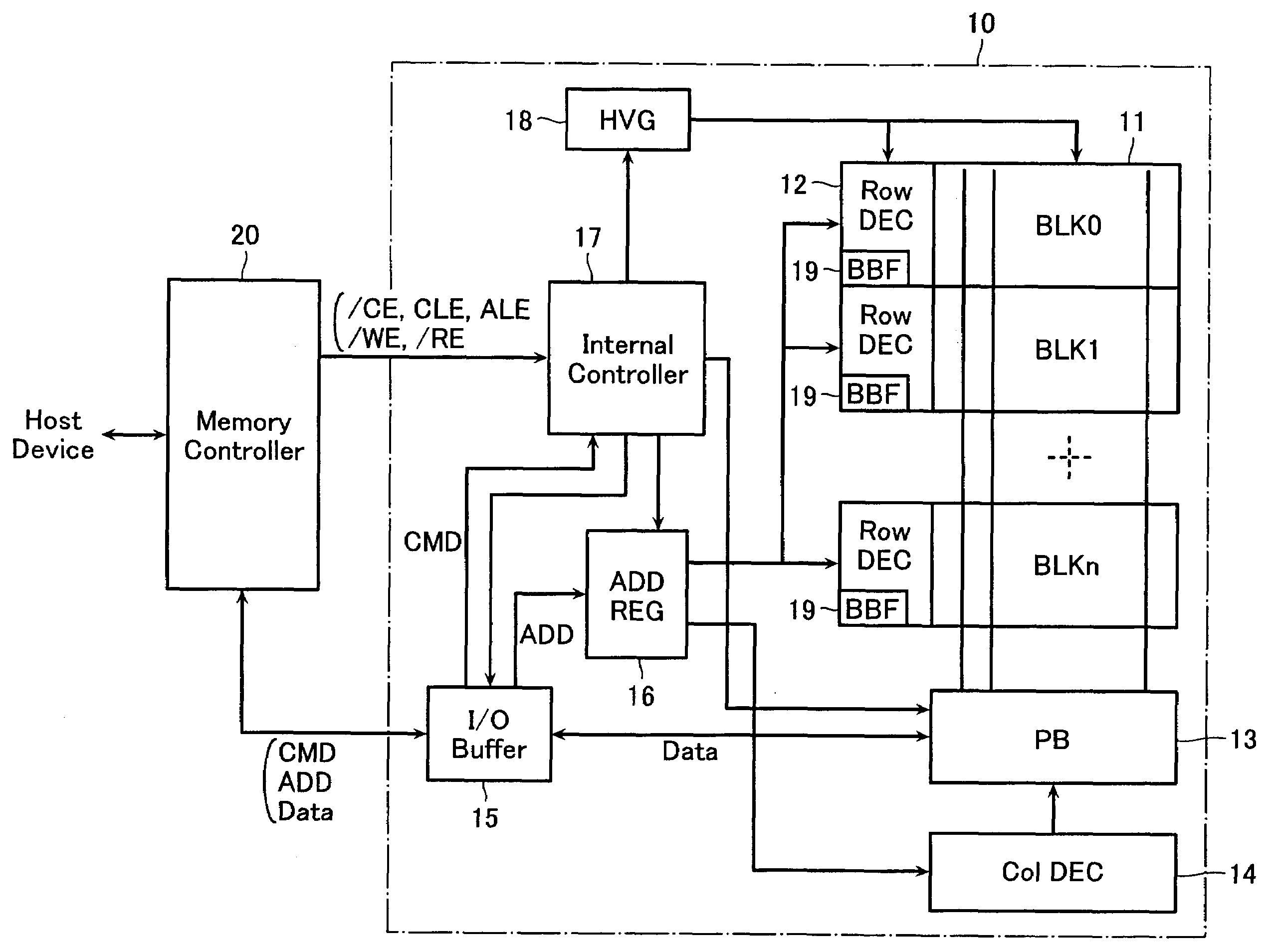
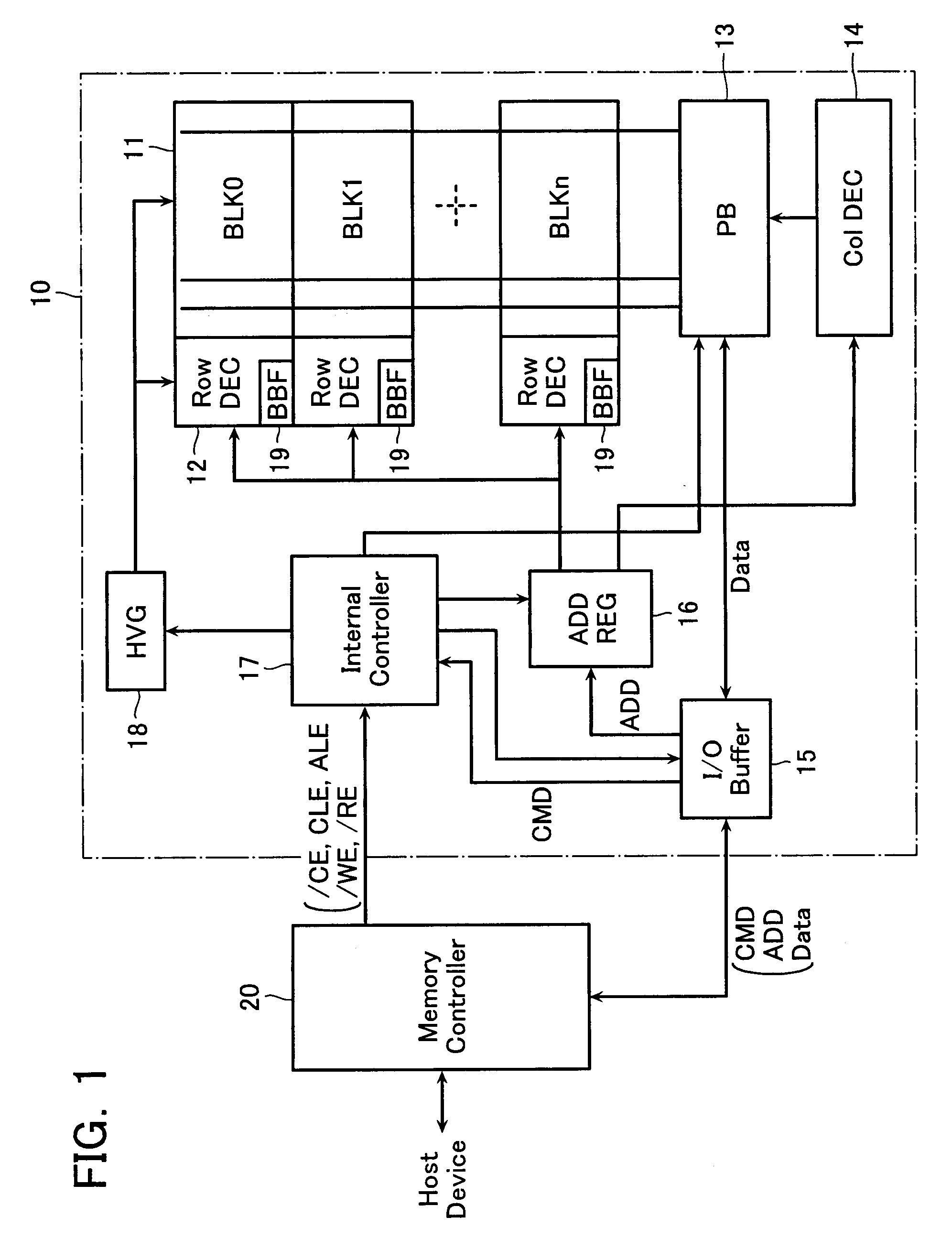
[0032]FIG. 1 shows a NAND-type flash memory in accordance with an embodiment. Flash memory chip 10 is packaged together with an external memory controller 20 for controlling it.

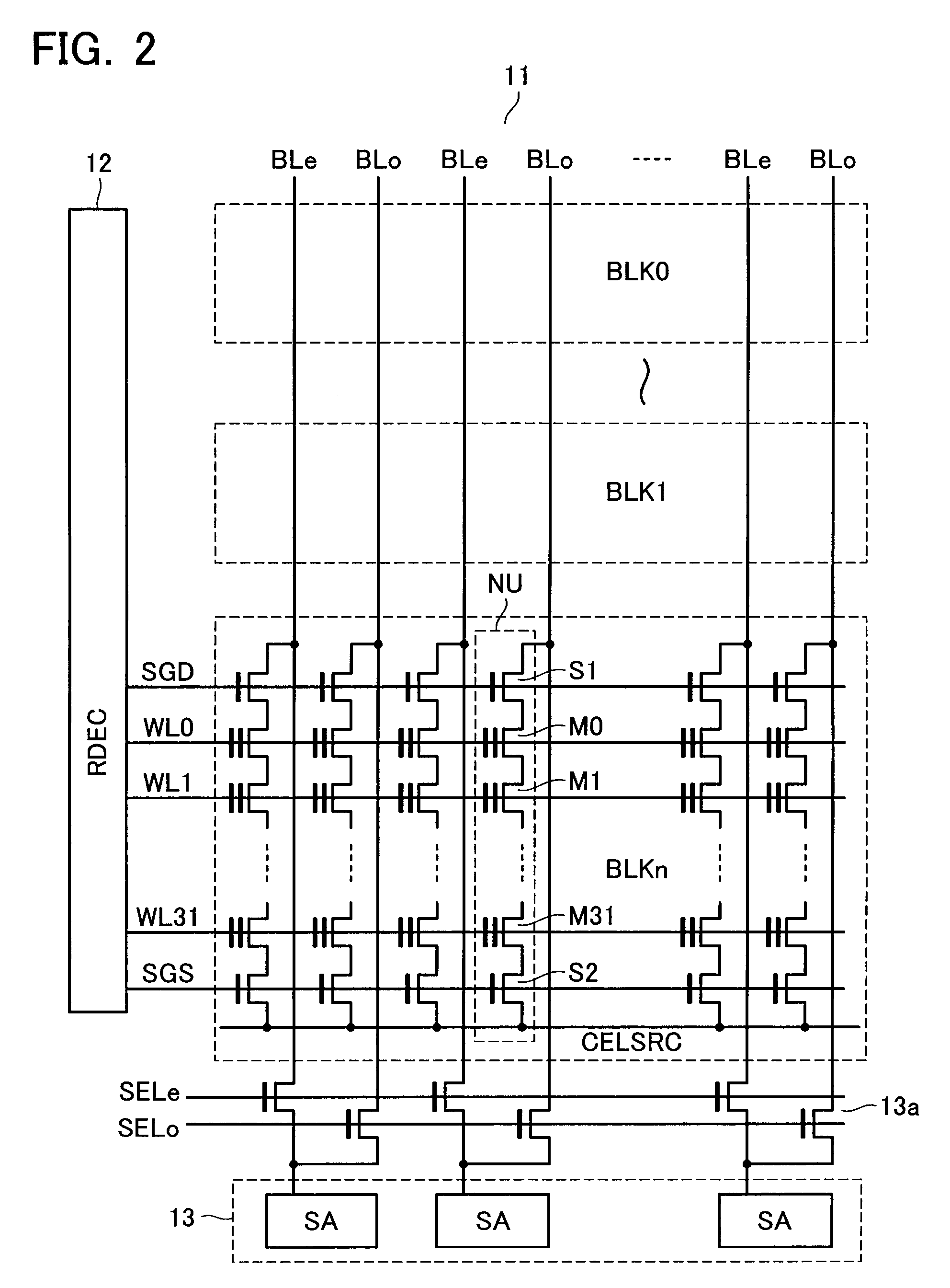
[0033]Flash memory chip 10 has cell array 11, row decoder 12 for selecting a word line thereof, page buffer 12 coupled to a bit line and used for reading and writing a page data and column decoder 14 for selecting a column. The cell array 11 is, as shown in FIG. 2, formed of multiple NAND cell units (or NAND strings) NU arranged therein.

[0034]The NAND cell unit NU has a plurality of electrically rewritable and non-volatile memory cells MC0-MC31 connected in series. Disposed at the both ends of the NAND cell unit NU are select gate transistors S1 and S2, which are used for coupling the unit to a bit line BL and a common source line CELSRC, respectively.

[0035]Control gates of the memory cells MC0...


PUM


Abstract

A non-volatile semiconductor memory device includes: a memory chip configured to be electrically rewritable and store such multi-level data as being defined by n-bits/cell (where n≧2); and a memory controller configured to control read and write of the memory chip, wherein the operation mode of the memory chip is changed from n-bits/cell to m-bits/cell (where m<n) when the number of late-generated defective areas is over a certain threshold value.

Description

CROSS-REFERENCE TO RELATED APPLICATION[0001]This application is based on and claims the benefit of priority from the prior Japanese Patent Application No. 2006-307692, filed on Nov. 14, 2006, the entire contents of which are incorporated herein by reference.BACKGROUND OF THE INVENTION[0002]1. Field of the Invention[0003]This invention relates to a non-volatile semiconductor memory device serving for storing multi-level data.[0004]2. Description of the Related Art[0005]A NAND-type flash memory is known as one of electrically rewritable and non-volatile semiconductor memories (EEPROMs). In the NAND-type flash memory, multiple memory cells are connected in series in such a manner that adjacent two memory cells share a source / drain region. Therefore, the unit cell area is small, and it is easy to increase the memory capacity.[0006]Recently, in the many kinds of mobile devices, there is a great demand for the NAND-type flash memory for storing music data and image data. Under this situat...

Claims


Application Information

Patent Timeline
IPC IPC(8): G11C16/04
CPCG11C11/5621G11C2211/5641G11C29/88G11C16/349G11C16/02G11C16/04G11C16/10
Inventor SHIRAKAWA, MASANOBU
Owner KK TOSHIBA
Why Eureka
Try Eureka