Technique for aging induced performance drift compensation in an integrated circuit

a technology of performance drift and integrated circuit, which is applied in the field of integrated circuits, can solve the problems of low gain of certain sensitive analog circuits, instability of high-performance pmos transistors, and reduced transistor's ability to drive curren

Active Publication Date: 2008-05-22
TEXAS INSTR INC
View PDF3 Cites 35 Cited by
  • Summary
  • Abstract
  • Description
  • Claims
  • Application Information

AI Technical Summary

Problems solved by technology

High performance PMOS transistors exhibit instability after voltage / temperature aging.
If a transistor's threshold voltage increases even slightly, the transistor's ability to drive current may be reduced sufficiently that a sensitive digital logic circuit in which the transistor is operating will slow down substantially or no longer function properly and the gain of certain sensitive analog circuits may be degraded.
This can disrupt the proper functioning of the entire integrated circuit.
The threshold voltage of a PMOS transistor can change over time due to NBTI instability induced aging.
Generally, NBTI induced aging affects PMOS pull-up performance and CHC related aging degrades NMOS pull-down performance.
The product performance drift can also manifest in increasing the delay of the critical path in a chip and hence can result in leading to functional failures.
This includes increasing the channel length of the nMOS device or stacking it with another device; both of these, however, can come with penalties—either in area or in performance.
However, this technique does not provide an individual handle on a PMOS device.
Further, this technique applies the same increased operating voltage VDD to both PMOS and NMOS transistors in the integrated circuit even though they degrade at different rates due to aging, which can significantly affect the integrated circuit properties by skewing the beta ratio.
Furthermore, increasing operating voltage VDD can result in further performance degradation as it is one primary reason for degradation of circuits.
Hence, an increment in VDD over the lifetime also risks an accelerated aging of the integrated circuit.
In addition, it also poses an increase in leakage power over the circuit lifetime.
Such compensation schemes are costly in terms of the area and also generally do not guarantee constant / drift-less performance over the circuit lifetime.
Thus, the existing schemes to determine the impact of hot carrier and NBTI induced aging on the performance of CMOS circuits and to recover the degraded performance are costly and inefficient.

Method used


Image

  • Technique for aging induced performance drift compensation in an integrated circuit
  • Technique for aging induced performance drift compensation in an integrated circuit
  • Technique for aging induced performance drift compensation in an integrated circuit

Examples


Embodiment Construction

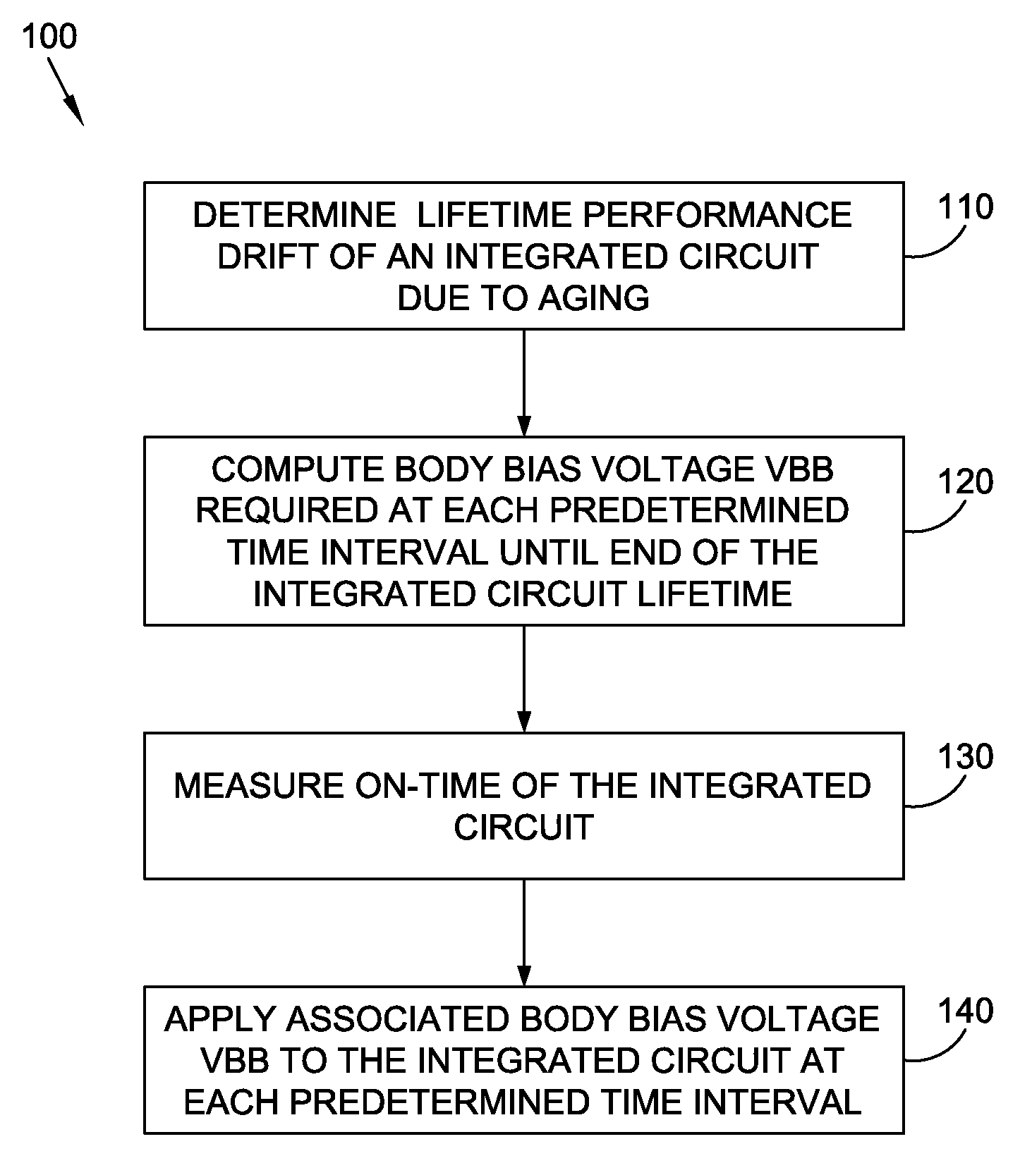
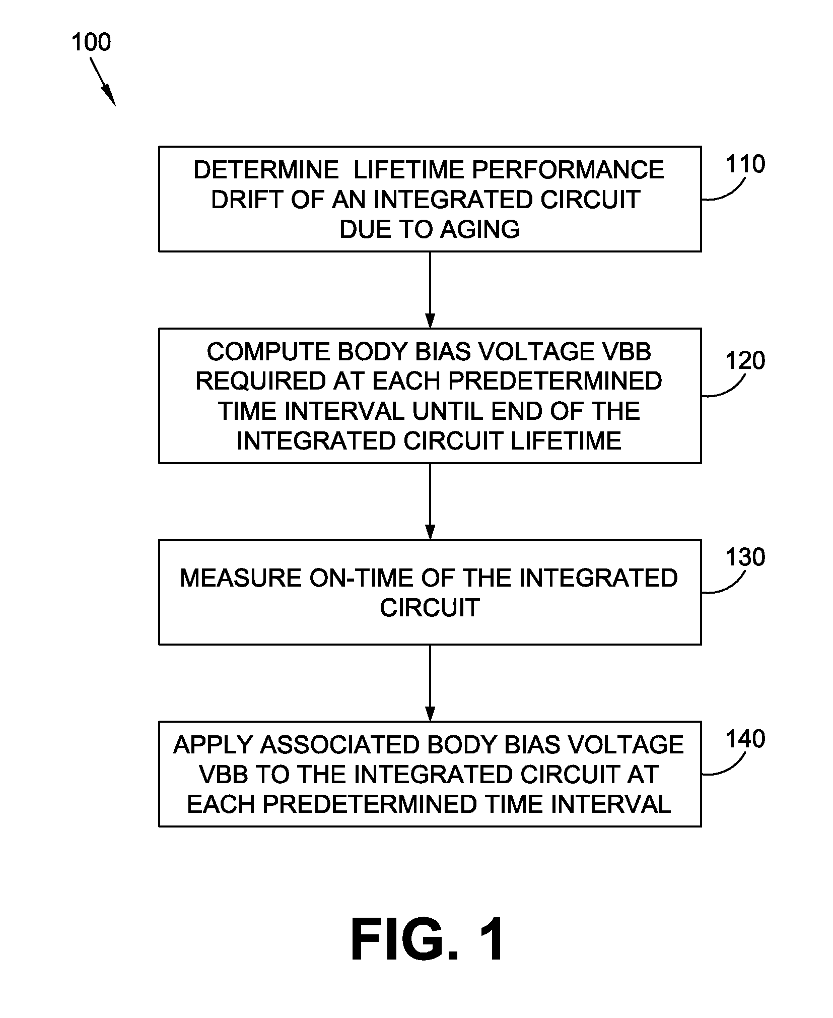
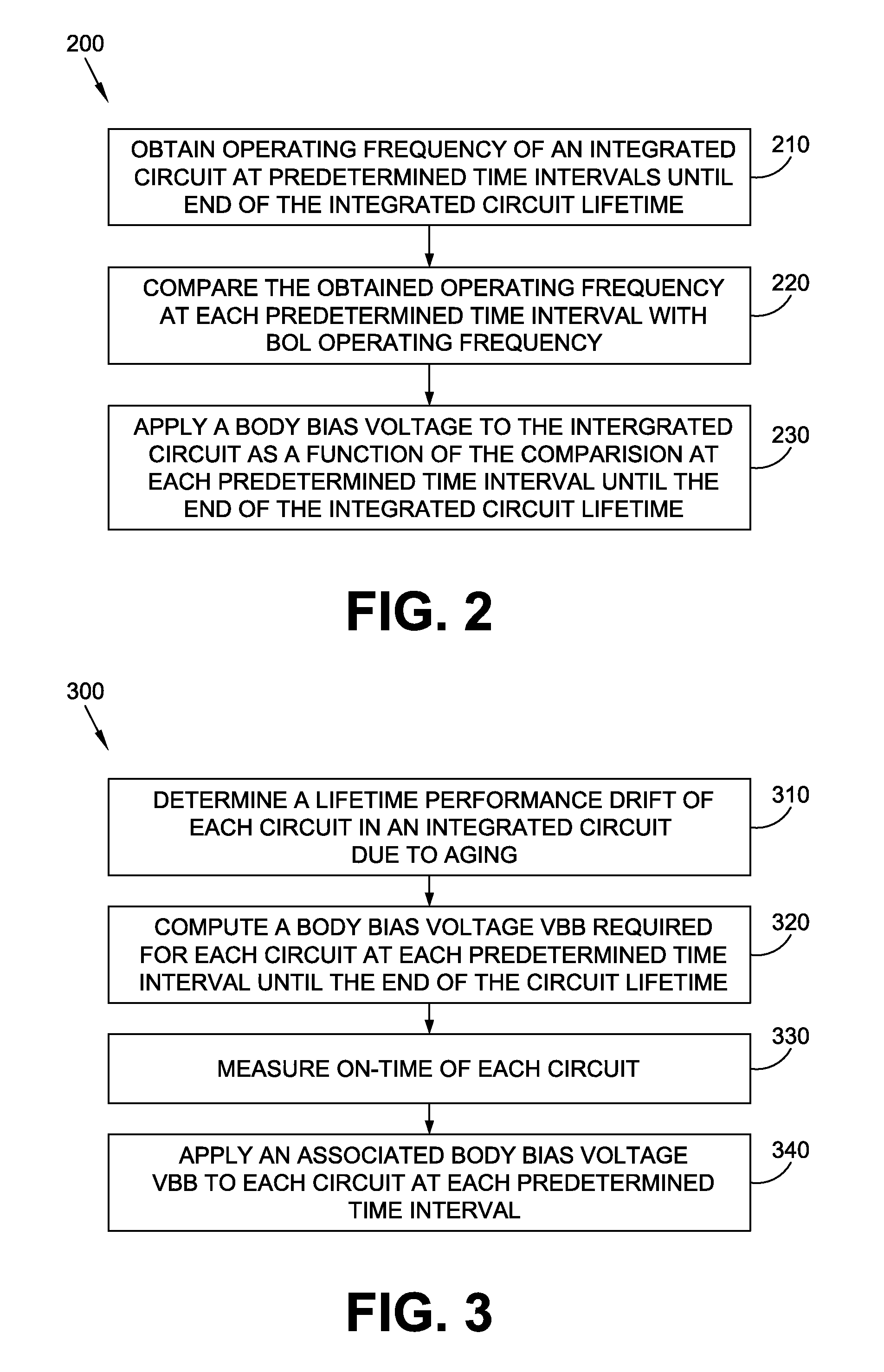
[0021]In the following detailed description of the embodiments of the invention, reference is made to the accompanying drawings that form a part hereof, and in which are shown by way of illustration specific embodiments in which the invention may be practiced. These embodiments are described in sufficient detail to enable those skilled in the art to practice the invention, and it is to be understood that other embodiments may be utilized and that changes may be made without departing from the scope of the present invention. The following detailed description is, therefore, not to be taken in a limiting sense, and the scope of the present invention is defined only by the appended claims.

[0022]The term “reliability simulations” refers to performing simulations of the integrated circuit by using Berkeley Reliability Tools (BERT) like techniques that are relevant for hot carrier and NBTI induced aging. Also, the term “performing silicon level measurements at accelerated stress condition...


PUM


Abstract

An improved compensation circuit that compensates for lifetime performance drifts due to aging of integrated circuits to improve the circuit performance. In one example embodiment, this is achieved by applying a body bias voltage VBB to the integrated circuit to compensate for the lifetime performance drift due to hot carrier and NBTI induced aging

Description

TECHNICAL FIELD OF THE INVENTION[0001]The present invention relates generally to integrated circuits, and more particularly relates to ways in which to improve circuit performance by compensating for the metal-oxide-semiconductor (MOS) transistor degradation due to aging.BACKGROUND OF THE INVENTION[0002]Integrated circuits based on complementary metal-oxide semiconductor (CMOS) transistor technology are widely used in modern electronic systems. The proper performance of CMOS integrated circuits is often critically dependent on the stable operation of its MOS transistors. Even relatively small changes in transistor performance can have a strong impact on the operation of sensitive circuitry on a high performance CMOS chip.[0003]The operation of a transistor can be significantly affected by changes in the transistor's threshold voltage due to aging induced by hot carrier, which is also referred to as CHC (channel hot carrier), and Negative Bias Temperature Instability (NBTI). High per...

Claims


Application Information

Patent Timeline
Patent Type & Authority Applications(United States)
IPC IPC(8): H01L23/58G01R31/27H01L27/00
CPCH03L1/00G01R31/2855
Inventor JAIN, PALKESHMAIR, HUGH THOMAS
Owner TEXAS INSTR INC
Why Eureka
Try Eureka