Light emission device and display device

Inactive Publication Date: 2008-05-22
SAMSUNG SDI CO LTD
View PDF4 Cites 19 Cited by
  • Summary
  • Abstract
  • Description
  • Claims
  • Application Information

AI Technical Summary

Benefits of technology

[0008]The present invention provides a light emission device and a display device using the light emission device as a light source, in which the light emission device can

Problems solved by technology

However, as light passes through the optical members, much light is lost.
Therefore, the CCFL and LED type light emission devices have relat

Method used


Image

  • Light emission device and display device
  • Light emission device and display device
  • Light emission device and display device

Examples


Example

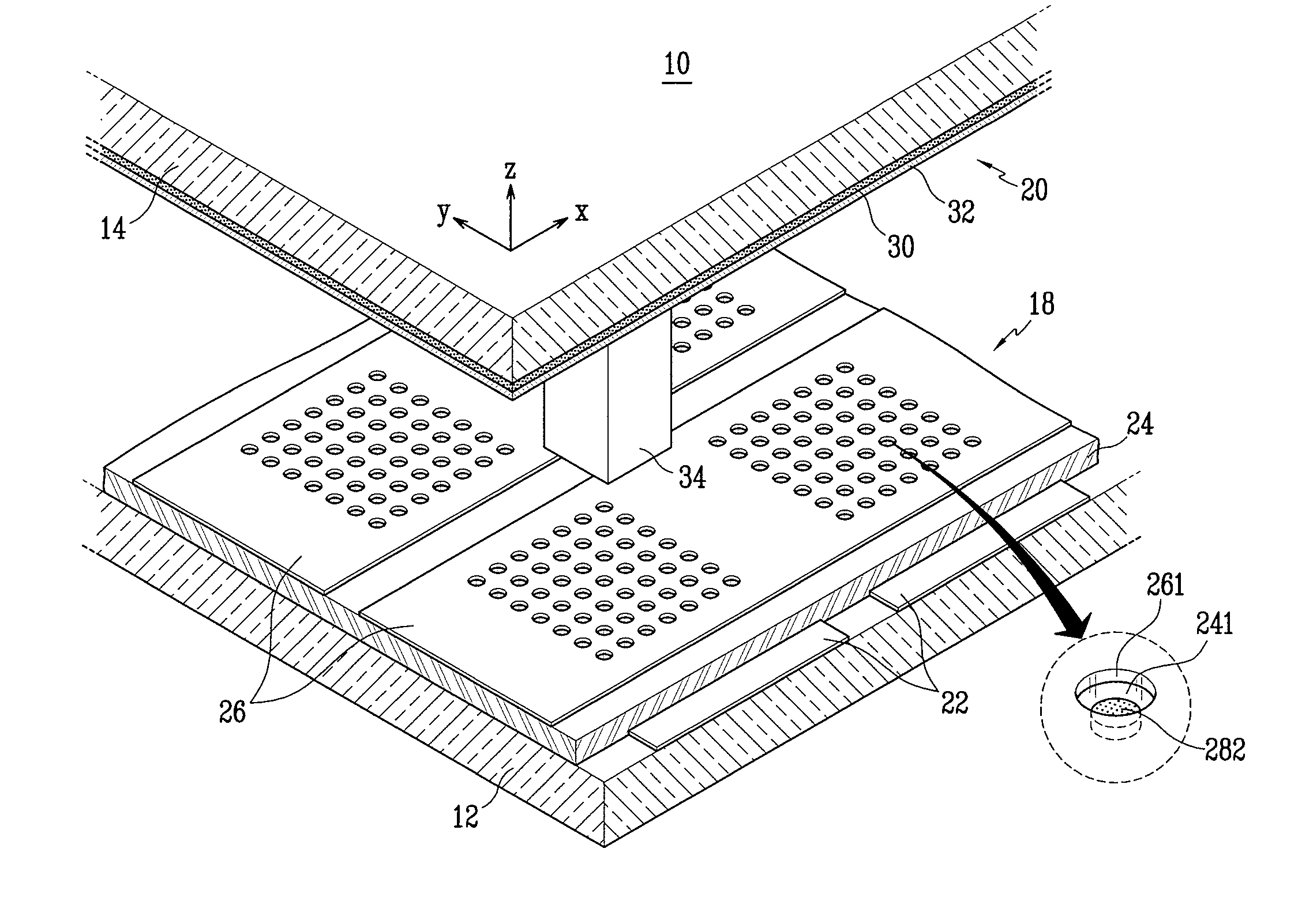
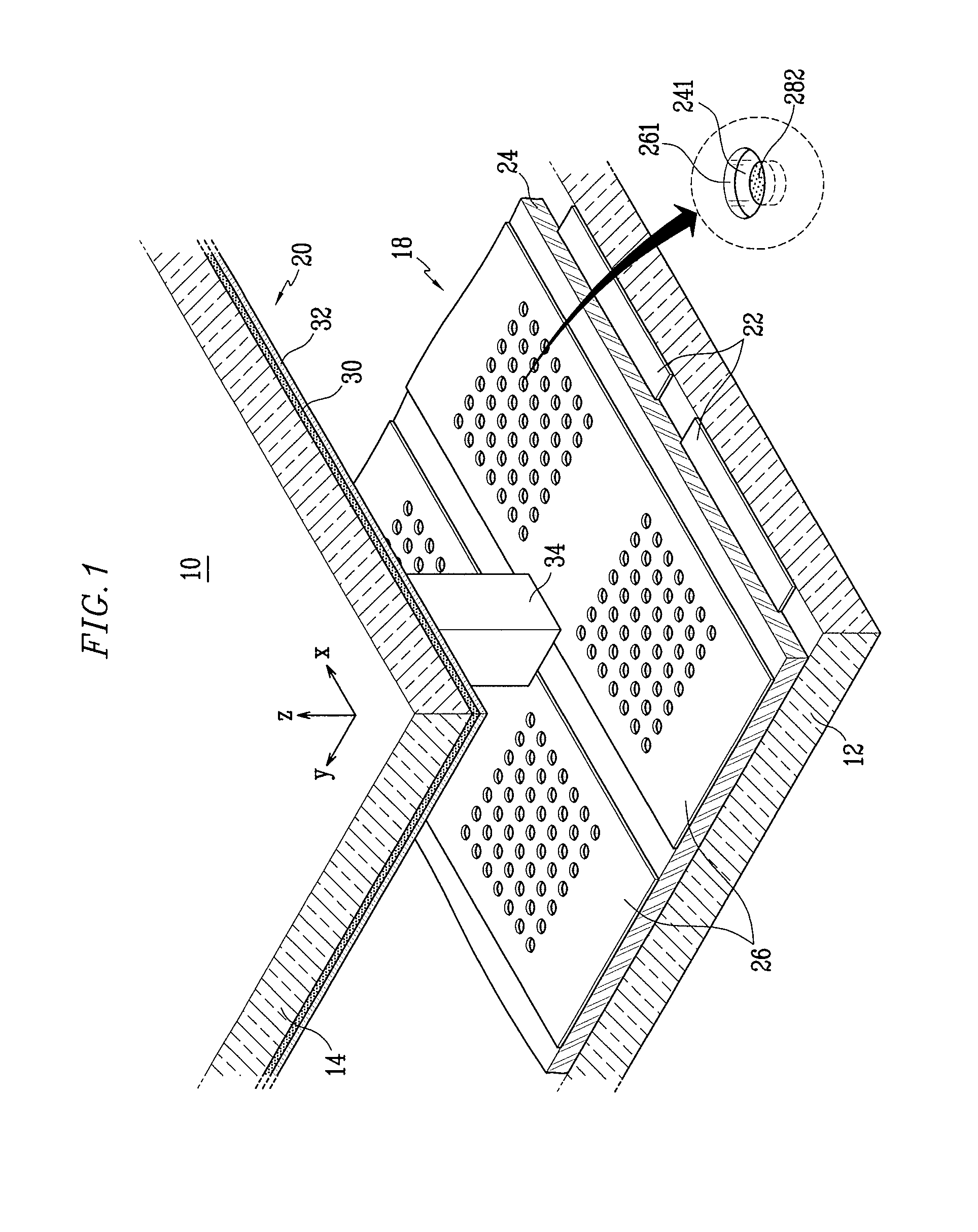
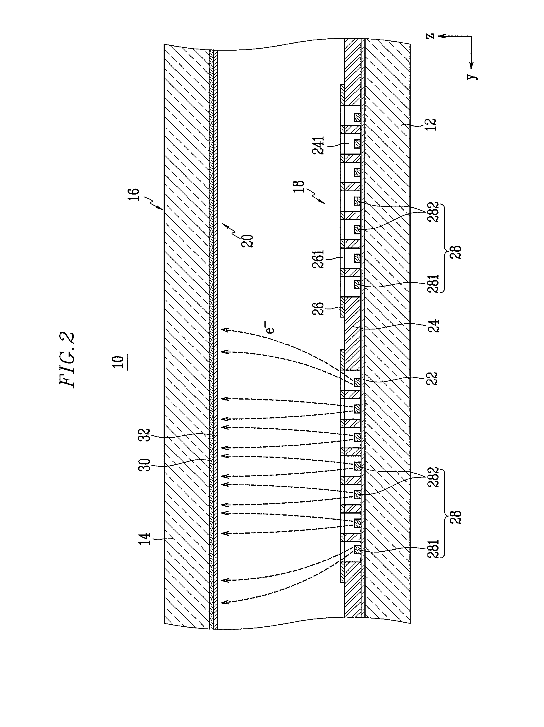
[0027]Referring to FIG. 1 and FIG. 2, a light emission device 10 of an exemplary embodiment includes first and second substrates 12, 14 facing each other in parallel at a predetermined interval. A sealing member (not shown) is provided between the first and second substrates 12, 14 to seal them together and thus form a vacuum vessel 16. The interior of the vacuum vessel 16 is kept to a degree of vacuum of about 10−6 Torr.

[0028]Inside the sealing member, the first and second substrates 12, 14 may be divided into an active area substantially emitting visible light and an inactive area surrounding the active area. An electron emission unit 18 for emitting electrons is provided on an inner surface of the first substrate 12 at the active area and a light emission unit 20 for emitting visible light is provided on an inner surface of the second substrate 14 at the active area.

[0029]The electron emission unit 18 includes cathode electrodes 22 arranged in a stripe pattern extending in a dire...


PUM


Abstract

A light emission device and display device utilizing the light emission device are provided. The light emission device includes first and second substrates facing each other. Cathode electrodes are arranged on an inner surface of the first substrate. Gate electrodes are arranged above and crossing the cathode electrodes. The gate electrodes have a plurality of openings at crossing regions of the gate electrodes and the cathode electrodes. Electron emission regions are formed on the cathode electrodes in the plurality of openings. A light emission unit is provided on an inner surface of the second substrate. At least one of the electron emission regions is located off of a center of a corresponding one of the plurality of openings.

Description

CROSS-REFERENCE TO RELATED APPLICATION[0001]This application claims priority to and the benefit of Korean Patent Application No. 10-2006-0114614 filed on Nov. 20, 2006 in the Korean Intellectual Property Office, the entire content of which is incorporated herein by reference.BACKGROUND OF THE INVENTION[0002]1. Field of the Invention[0003]The present invention relates to a light emission device and a display device, and more particularly, to a light emission device with enhanced light emission uniformity in an active area, and a display device using the light emission device as a light source.[0004]2. Description of the Related Art[0005]A display device having a passive-type display panel, such as a liquid crystal display panel, needs a light source for emitting light toward the display panel. Cold cathode fluorescent lamp (CCFL) type and a light emitting diode (LED) type light emission devices are generally used as the light source of the display device.[0006]Because the CCFL and LE...

Claims


Application Information

Patent Timeline
IPC IPC(8): H01J63/04
CPCH01J3/021H01J63/02H01J31/127H01J29/481G02F1/1335H01J1/30H01J1/304
Inventor KIM, BYOUNG-KUKLEE, JIN-HOKIM, HUN-SOO
Owner SAMSUNG SDI CO LTD
Why Eureka
Try Eureka