[0009]With the abovementioned method, a so-called pre-tilt angle is imparted to almost all of the liquid crystal molecules of the liquid crystal layer, as shown in FIG. 10, because the ultra-
violet light is irradiated to the entire surface of the board. Although the pre-tilt provided throughout the entire surface of the liquid crystal layer can improve the response speed against
voltage, slight light may be penetrated even in the undriven (black display) state. This increases the luminance of the black display, leading to a drop in contrast.
[0012]It is desirable to provide a
liquid crystal display enabling efficient improvement of the response speed against
voltage, while suppressing a drop in contrast, and provide a method of manufacturing the liquid
crystal display.
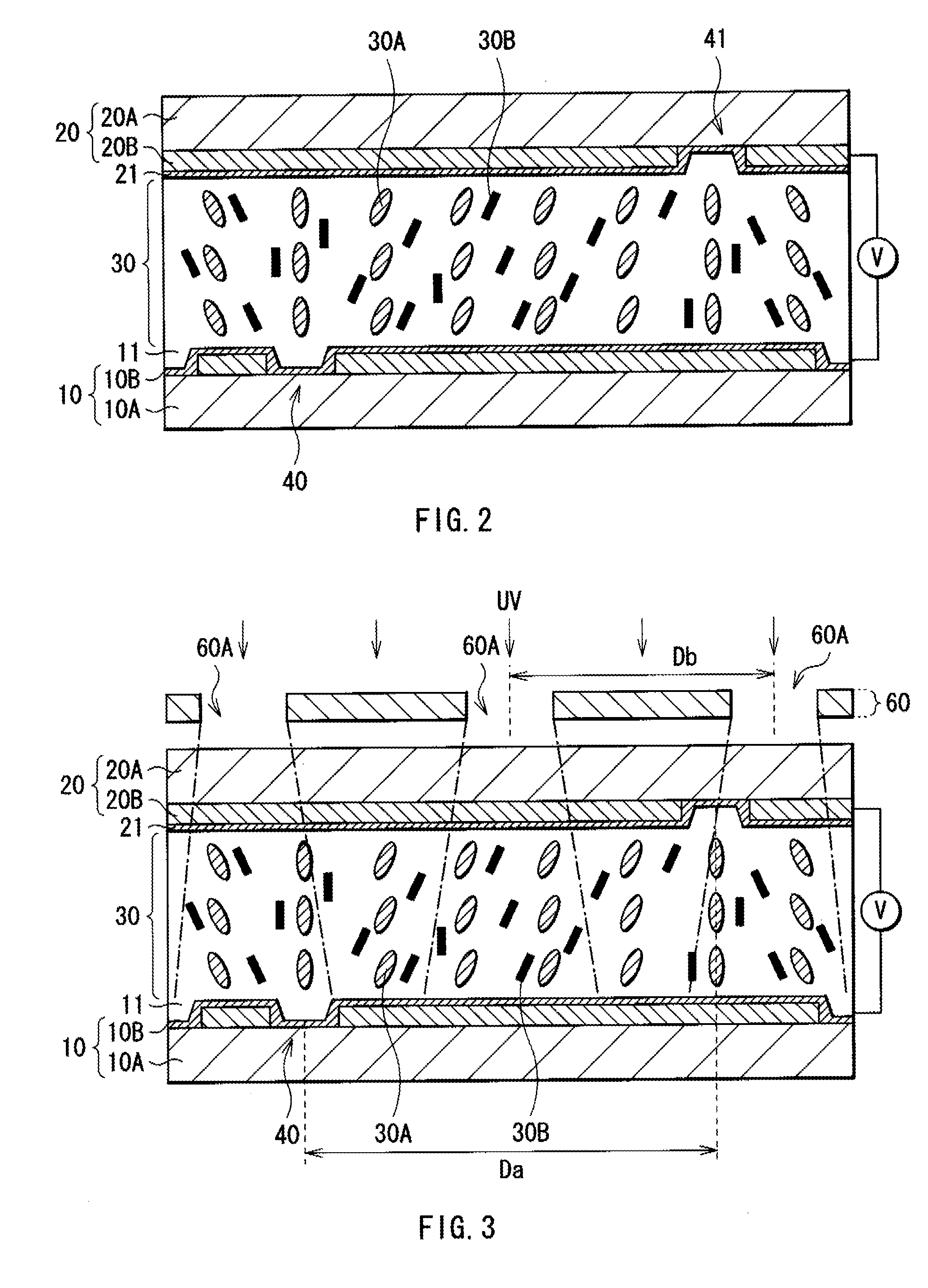
[0015]In the method of manufacturing the liquid
crystal display according to the present invention,
exposure to a region having a low response speed against voltage, between the gap of the pixel
electrode on one substrate and the gap of the pixel electrode on the other substrate, can be ensured by exposing the liquid crystal layer containing the
light curing material, through the light shielding film having the plurality of openings at spacing smaller than the spacing between the respective gaps of the pair of pixel electrodes, with a voltage applied between the pair of pixel electrodes having predetermined gaps. As a result, an obliquely aligned layer (the
light curing layer for obliquely aligning the liquid crystal molecules) can be formed in the exposed part. By the presence of the obliquely aligned layer, a pre-tilt angle can be imparted to the liquid crystal molecules in the region having the low response speed. That is, without any precise alignment between the
mask for exposure and the pixel electrodes slits, the pre-tilt angle can be imparted efficiently to the region having the low response speed. Here, because no obliquely aligned layer is formed in unexposed regions, no pre-tilt angle is imparted to liquid crystal molecules, and the liquid crystal molecules are aligned vertically to the substrates. However, no issues will occur because even if it corresponds to the slit-
proximate region, this region naturally has a high response speed. In the unexposed regions, the liquid crystal molecules are aligned vertically to the substrates, and this is advantageous for black display.
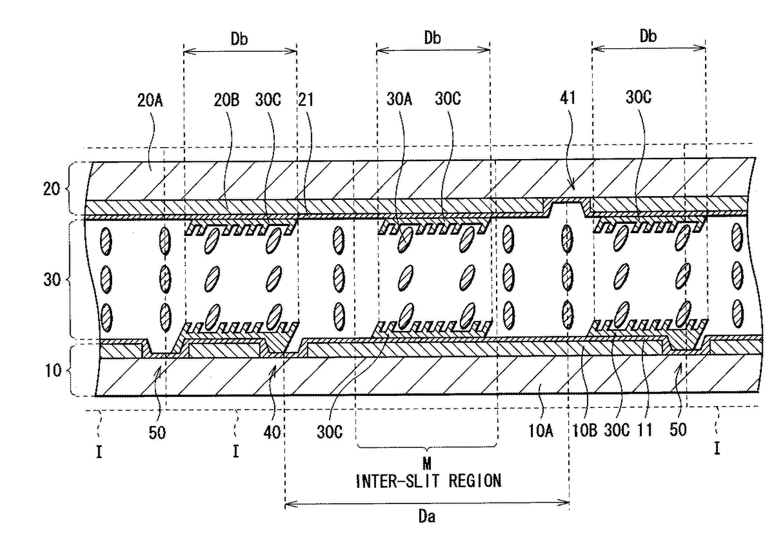
[0016]In the liquid
crystal display according to the present invention, between the pair of oppositely disposed substrates, the liquid crystal layer is sealed with the pair of pixel electrodes having the predetermined gaps in between. The liquid crystal layer is disposed in the plane directions of the substrates at spacing smaller than spacing between the respective gaps of the pair of pixel electrodes. The liquid crystal layer has the light curing layer for obliquely aligning liquid crystal molecules. This ensures that the light curing layer is provided for the region having the low response speed against voltage in the liquid crystal layer. The presence of the light curing layer ensures that the liquid crystal molecules in the region having the low response speed are held in the pre-tilt state. In the region having no light curing layer, the liquid crystal molecules cannot be held in the pre-tilt state and are aligned vertically to the substrates. However, no issues will occur because if it corresponds to the slit-
proximate region, this region naturally has a high response speed. In the unexposed regions, the liquid crystal molecules are aligned vertically to the substrates, and this is advantageous for black display.
[0017]The method of manufacturing the liquid crystal display of the present invention includes the steps of: forming pixel electrodes on inside surfaces of a couple of substrates facing each other, each of the pixel electrodes having gaps; sealing, between the couple of substrates with the pixel electrodes formed, a liquid crystal layer containing a light curing material; and exposing the liquid crystal layer through use of a light shielding film having a plurality of openings, under a voltage applied between a pair of pixel electrodes facing each other on the couple of substrates. Particularly, the gaps are alternately disposed to form a staggered arrangement between the pair of pixel electrodes, and spacing between adjacent openings of the light shielding film is smaller than spacing, in a
substrate surface direction, between the gap of a pixel electrode on one substrate and the gap of a pixel electrode on the other substrate. This permits manufacture of a liquid crystal display enabling efficient improvement of the response speed against voltage, while suppressing a drop in contrast.
[0018]The liquid crystal display of the present invention includes: a couple of substrates facing each other; pixel electrodes formed on inside surfaces of a couple of substrates, each of the pixel electrodes having gaps; and a liquid crystal layer sealed between the couple of substrates with the pixel electrodes formed. The gaps are alternately disposed to form a staggered arrangement between the pair of pixel electrodes. The liquid crystal layer has pre-tilt regions where liquid crystal molecules are tilted, spacing between adjacent pre-tilt regions being smaller than spacing, in a
substrate surface direction, between the gap of a pixel electrode on one substrate and the gap of a pixel electrode on the other substrate. This enables efficient improvement of the response speed against voltage, while suppressing a drop in contrast.

