Stress measurement and stress balance in films

a stress measurement and stress balance technology, applied in the direction of semiconductor/solid-state device testing/measurement, coating, chemical vapor deposition coating, etc., can solve the problems of poor luminescence of devices, impeded practical fabrication, and difficulty in efficient p-doping of such materials

Inactive Publication Date: 2008-05-29
APPLIED MATERIALS INC
View PDF1 Cites 254 Cited by
  • Summary
  • Abstract
  • Description
  • Claims
  • Application Information

AI Technical Summary

Problems solved by technology

While some modestly successful efforts had previously been made in the production of blue LEDs using SiC materials, such devices suffered from poor luminescence as a consequence of the fact that their electronic structure has an indirect bandgap.
While the feasibility of using GaN to create photoluminescence in the blue region of the spectrum has been known for decades, there were numerous barriers that impeded their practical fabrication.
These included the lack of a suitable substrate on which to grow the GaN structures, generally high thermal requirements for growing GaN that resulted in various thermal-convection problems, and a variety of difficulties in efficient p-doping such materials.
The use of sapphire as a substrate was not completely satisfactory because it provides approximately a 15% lattice mismatch with the GaN.
While some improvements have thus been made in the manufacture of such compound nitride semiconductor devices, it is widely recognized that a number of deficiencies yet exist in current manufacturing processes.
Moreover, the high utility of devices that generate light at such wavelengths has caused the production of such devices to be an area of intense interest and activity.

Method used


Image

  • Stress measurement and stress balance in films
  • Stress measurement and stress balance in films
  • Stress measurement and stress balance in films

Examples


Embodiment Construction

1. Overview

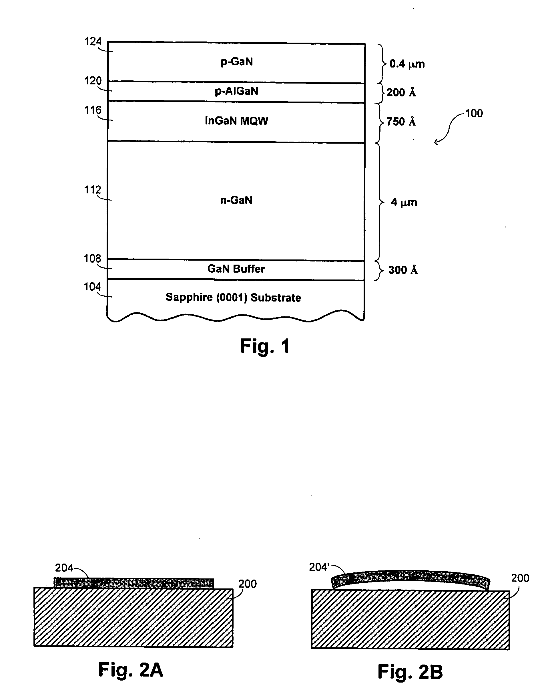
[0025]One of the difficulties mentioned above in fabricating nitride-based structures such as GaN structures is the accommodation of generally high thermal requirements for growth of GaN. Historically, this made the identification of a suitable substrate difficult, with the art more recently focusing on ways in which the use of sapphire Al2O3 may be accommodated. Sapphire is not an ideal substrate because there is a significant lattice mismatch with deposited nitride layers; in the specific case of GaN, this lattice mismatch is approximately 15%. While the use of a nitride buffer layer has been helpful in accommodating the lattice mismatch, both the lattice mismatch and other physical differences between the sapphire substrate and overlying nitride layer result in distortions of resulting structures.

[0026]One typical nitride-based structure is illustrated in FIG. 1 as a GaN-based LED structure 100. It is fabricated over a sapphire (0001) substrate 104. An n-type GaN layer...


PUM

PropertyMeasurementUnit
temperatureaaaaaaaaaa
thicknessaaaaaaaaaa

Abstract

Methods and systems are provided of fabricating a compound nitride semiconductor structure. A substrate is disposed within a processing chamber into which a group-III precursor and a nitrogen precursor are flowed. A layer is deposited over the substrate with a thermal chemical-vapor-deposition process using the precursors. The substrate is transferred to a transfer chamber where a temperature and a curvature of the layer are measured. The substrate is then transferred to a second processing chamber where a second layer is deposited.

Description

BACKGROUND OF THE INVENTION[0001]The history of light-emitting diodes (“LEDs”) is sometimes characterized as a “crawl up the spectrum.” This is because the first commercial LEDs produced light in the infrared portion of the spectrum, followed by the development of red LEDs that used GaAsP on a GaAs substrate. This was, in turn, followed by the use of GaP LEDs with improved efficiency that permitted the production of both brighter red LEDs and orange LEDs. Refinements in the use of GaP then permitted the development of green LEDs, with dual GaP chips (one in red and one in green) permitting the generation of yellow light. Further improvements in efficiency in this portion of the spectrum were later enabled through the use of GaAlAsP and InGaAlP materials.[0002]This evolution towards the production of LEDs that provide light at progressively shorter wavelengths has generally been desirable not only for its ability to provide broad spectral coverage but because diode production of shor...

Claims


Application Information

Patent Timeline
Patent Type & Authority Applications(United States)
IPC IPC(8): H01L21/66C23C16/00
CPCH01L21/0242H01L21/02458H01L21/0254H01L33/007H01L22/12H01L22/20H01L21/0262
Inventor BOUR, DAVIDNIJHAWAN, SANDEEPWASHINGTON, LORI D.SMITH, JACOB W.
Owner APPLIED MATERIALS INC
Why Eureka
Try Eureka