
Semiconductor device

Inactive Publication Date: 2008-06-05
RENESAS ELECTRONICS CORP
View PDF7 Cites 8 Cited by
  • Summary
  • Abstract
  • Description
  • Claims
  • Application Information

AI Technical Summary

Benefits of technology

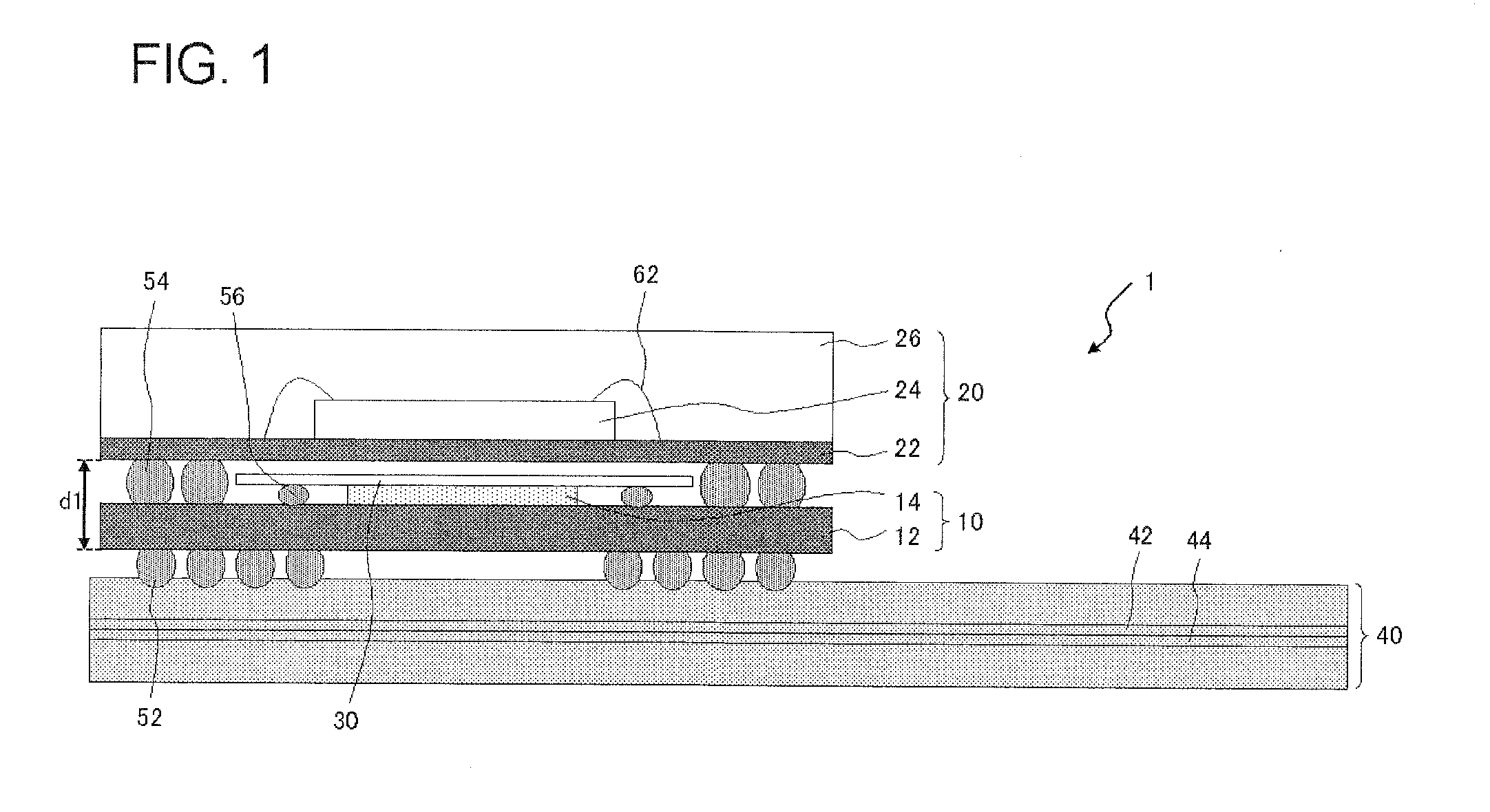
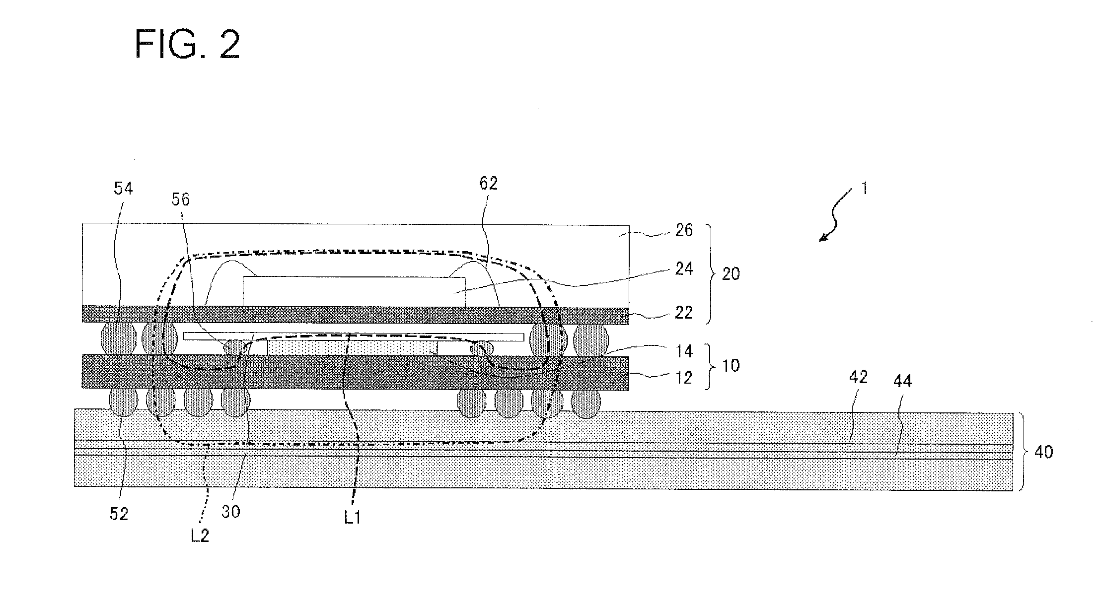
[0009]In such aspect of the present invention, the electrically conductive plate having a fixed potential is provided between the first and the second semiconductor packages. This allows providing a stable reference potential, similarly as in a case that a ground plane (or a power source plane) is disposed in vicinity of the interconnect substrate of the second semiconductor package (second interconnect substrate). Thus, a stable intrinsic impedance of the interconnect in the second interconnect substrate can also be provided.
[0010]According to the present invention, a semiconductor device having a POP structure, which is suitable for providing a stable intrinsic impedance of an interconnect in an interconnect substrate that is included in an upper semiconductor package, is achieved.

Problems solved by technology

Such increased distance causes unstable reference potential, resulting in unstable intrinsic impedance of interconnects in the interconnect substrate 132.

Method used


Image

  • Semiconductor device
  • Semiconductor device
  • Semiconductor device

Examples


first embodiment

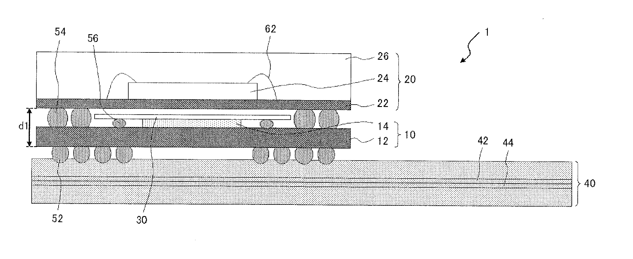
[0023]FIG. 1 is a cross-sectional view showing the first embodiment of a semiconductor device by the present invention. A semiconductor device 1 includes a semiconductor package 10 (first semiconductor package), a semiconductor package 20 (second semiconductor package) and an electrically conductive plate 30. The semiconductor package 10 includes an interconnect substrate 12 (first interconnect substrate) and a semiconductor chip 14 (first semiconductor chip). The interconnect substrate 12 is substantially flat. The semiconductor chip 14 is mounted on the interconnect substrate 12 by a flip-chip bonding. The semiconductor package 10 is mounted on a mounting board 40 via conductive bumps 52. The mounting board 40 includes a ground (hereinafter referred to as “GND”) plane 42 and a power source plane 44. In addition to above, the GND plane 42 is electrically isolated from the power source plane 44 by an insulating layer that is not shown.

[0024]The semiconductor package 20 is disposed o...

second embodiment

[0039]FIG. 3 is a cross-sectional view, illustrating second embodiment of a semiconductor device according to the present invention. A semiconductor device 2 includes a holding substrate 70, which is capable of holding the conductive plate 30, in addition to the semiconductor packages 10 and 20 and the conductive plate 30. The holding substrate 70 is coupled to the interconnect substrate 12 via conductive bumps 58. The semiconductor package 20 is, in turn, mounted on the holding substrate 70 via conductive bumps 54. This provides a configuration, in which the semiconductor package 10 is coupled to the semiconductor package 20 via the holding substrate 70. Other configurations of the semiconductor device 2 are similar to that of the semiconductor device 1 shown in FIG. 1. However, an illustrations of the semiconductor chip 24, the mounting board 40 or the like (see FIG. 1) is not presented in FIG. 3.

[0040]According to the semiconductor device 2 having such configuration, a larger dim...

third embodiment

[0041]FIG. 4 is a cross-sectional view, illustrating third embodiment of a semiconductor device according to the present invention. In a semiconductor device 3, three semiconductor packages are stacked on a mounting board 40. More specifically, a semiconductor package 90 having an interconnect substrate 92 and a semiconductor chip 94 interposes between the semiconductor package 10 and the semiconductor package 20. The semiconductor package 90 is mounted on the semiconductor package 10 via conductive bumps 55. The semiconductor package 20 is, in turn, mounted on the semiconductor package 90 via the conductive bumps 54. Conductive plates 30a and 30b are provided between the semiconductor package 10 and the semiconductor package 20. More specifically, the conductive plate 30a is provided between the semiconductor package 20 and the semiconductor package 90, and the conductive plate 30b is provided between the semiconductor package 90 and the semiconductor package 10. The conductive pla...


PUM


Abstract

In one embodiment, provided is a semiconductor device including a first semiconductor package, a second semiconductor package and a conductive plate. The first semiconductor package includes a first interconnect substrate and a first semiconductor chip. The second semiconductor package includes a second interconnect substrate and a second semiconductor chip, and is stacked on the first semiconductor package. The conductive plate is provided between the first semiconductor package and the second semiconductor package. The conductive plate is electrically coupled to the GND plane of the mounting board, so that a fixed potential is provided. The distance from the lower surface of the first interconnect substrate to the lower surface of the second interconnect substrate is larger than a total of a thickness of the first interconnect substrate, a thickness of the first semiconductor chip and a thickness of the conductive plate.

Description

[0001]This application is based on Japanese patent application No. 2006-327,297, the content of which is incorporated hereinto by reference.BACKGROUND[0002]1. Technical Field[0003]The present invention relates to a semiconductor device.[0004]2. Related Art[0005]FIG. 9 is a cross-sectional view, showing a conventional semiconductor device. A semiconductor device 100 has a package on package (POP) structure. More specifically, a semiconductor package 120 and a semiconductor package 130 are sequentially stacked on a mounting board 110. A semiconductor package 120 includes an interconnect substrate 122 and a semiconductor chip 124. Similarly, a semiconductor package 130 includes an interconnect substrate 132 and a semiconductor chip 134.[0006]Prior art literatures related to the present invention includeJapanese Patent Laid-Open No. 2000-174,204, Japanese Patent Laid-Open No. 2003-163,310, Japanese Patent Laid-Open No. 2002-271,101, Japanese Patent Laid-Open No. H8-51,127 (1996) and Jap...

Claims


Application Information

Patent Timeline
IPC IPC(8): H01L23/538
CPCH01L23/552H01L25/105H01L2924/3025H01L2924/30107H01L2225/1058H01L2225/1023H01L24/48H01L2224/48091H01L2224/48227H01L2924/3011H01L2924/00014H01L2924/00H01L2924/181H01L2224/16225H01L2924/15311H01L2924/00012H01L2224/45099H01L2224/45015H01L2924/207
Inventor SEKIGUCHI, TOMOHISA
Owner RENESAS ELECTRONICS CORP
Learn More