Antenna device

a technology of antennas and antennas, applied in the direction of antennas, antenna feed intermediates, antenna details, etc., can solve the problems of high loss of high frequency signal transmission, achieve good spacing, facilitate matching output impedance, and stabilize impedance

Inactive Publication Date: 2015-02-12
HITACHI METALS LTD
View PDF5 Cites 6 Cited by
  • Summary
  • Abstract
  • Description
  • Claims
  • Application Information

AI Technical Summary

Benefits of technology

[0097]The embodiment described above has the following functions and advantageous effects.
[0098](1) The regulating surface 312c of the second hole 312 regulates the movement of the projecting piece 41a or 42a inserted in the second hole 312 of the through-hole 31a toward the first opposite surface 311b, and can thereby maintain the good spacing between the connecting pin 8 joined to the built-in feed line 411 or 421 and the first opposite surface 311b of the first hole 311. This facilitates matching the output impedance of the central conductor 33 (the triplate line) and the input impedance of the antenna element 4.
[0099](2) The built-in feed line 411 or 421 on the projecting piece 41a or 42a of the antenna element 4 and the first ground plate 31 constitute the triplate structure between the first opposite surface 311b and the second opposite surface 312b parallel to each other of the through-hole 31a, and can thereby stabilize impedance and lower high frequency signal transmission loss in the connecting portion between the built-in feed line 411 or 421 and the central conductor 33, as compared with when a coaxial cable or the like is used therebetween.
[0100](3) The built-in feed line 411 or 421 of the antenna element 4 and the central conductor 33 are electrically connected together via the connecting pin 8, and can thereby ensure the simplification of the connecting structure between the built-in feed line 411 or 421 of the antenna element 4 and the central conductor 33 of the triplate line.
[0101](4) In the triplate structure in the through-hole 31a, the distance D4 between the connecting pin 8 and the first opposite surface 311b is configured as being greater than the thickness D3 (D4>D3) of the dielectric substrate 420, and the width direction dimension D1 of the connecting pin 8 is smaller than the width direction dimension D2 (D1<D2) of the built-in feed line 421 (the second connection pattern 421b), where the width direction is parallel to the first principal surface 420a of the dielectric substrate 420. The impedance matching can therefore be done with the width direction dimension D2 of the built-in feed line 421 (the second connection pattern 421b). Also, for example, even if the connecting pin 8 is tilted slightly relative to the vertical direction to the central conductor 33, the connecting pin 8 fits in the width direction dimension D2 of the built-in feed line 421 (the second connection pattern 421b). The impedance of the connecting portion between the built-in feed line 411 or 421 and the central conductor 33 is therefore stable.
[0102](5) The contact portion 71a of the radiating element connecting bracket 71 connected with the radiating element 412 or 422 of the antenna element 4 at least partially overlaps the built-in feed line 411 or 421 on the first principal surface 410a or 420a of the dielectric substrate 410 or 420 in the thickness direction of the dielectric substrate 410 or 420. That is, the high frequency signal transmission loss can be lowered by grounding adjacent to the connecting portion between the built-in feed line 411 or 421 and the central conductor 33.

Problems solved by technology

In the antenna device described in JP-A-2009-124403, due to the feeding portion configuration in which the feeding pin is soldered on the inner surface of the round hole formed in the mount with the coaxial cable or the like therebetween, no impedance matching in a connecting portion between the input side feeding portion and the output side built-in feed line is likely to occur, and high frequency signal transmission loss therein is high.

Method used


Image

  • Antenna device
  • Antenna device
  • Antenna device

Examples


Embodiment Construction

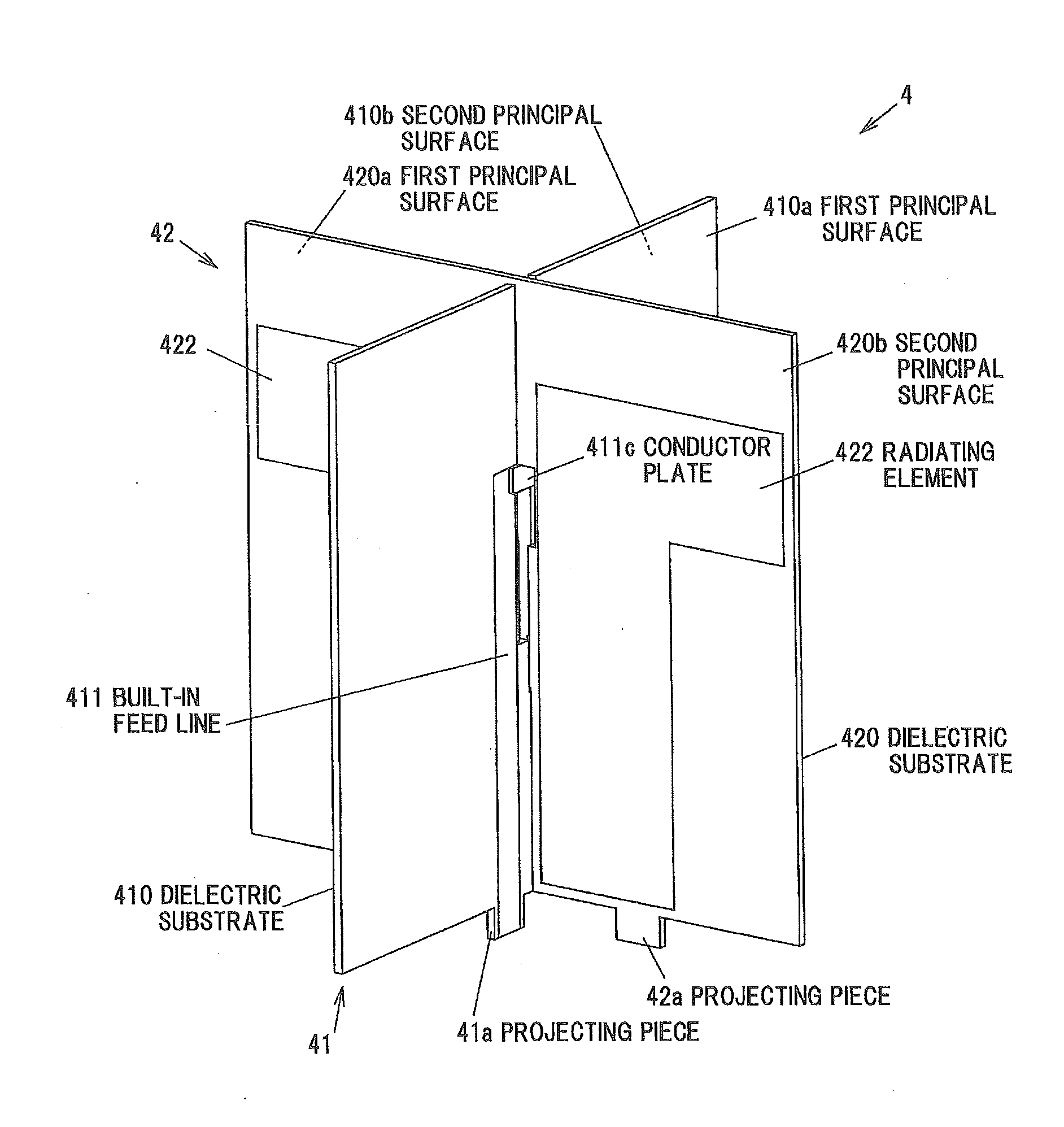
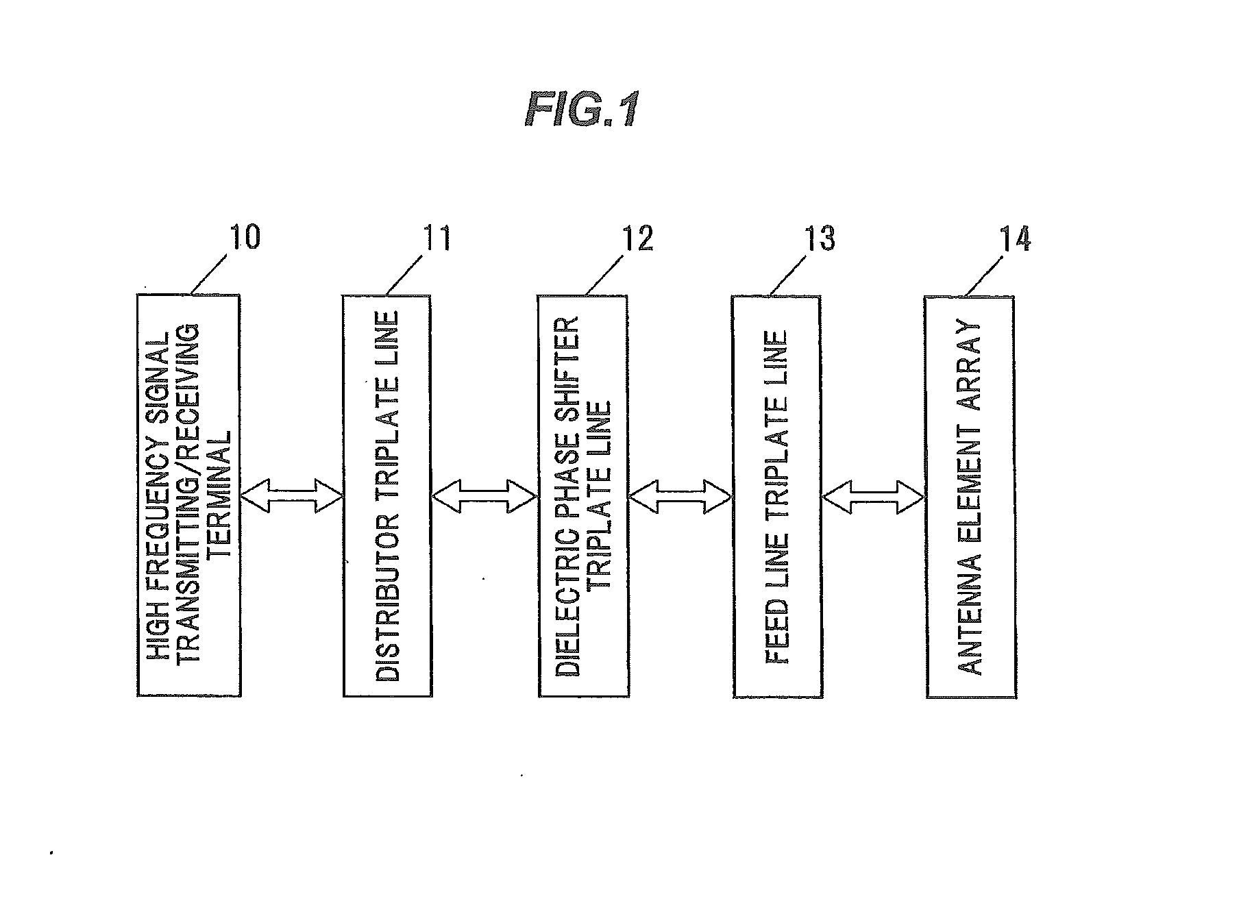
[0038]FIG. 1 is a block diagram showing a schematic configuration of an antenna device 1 in an embodiment according to the present invention.

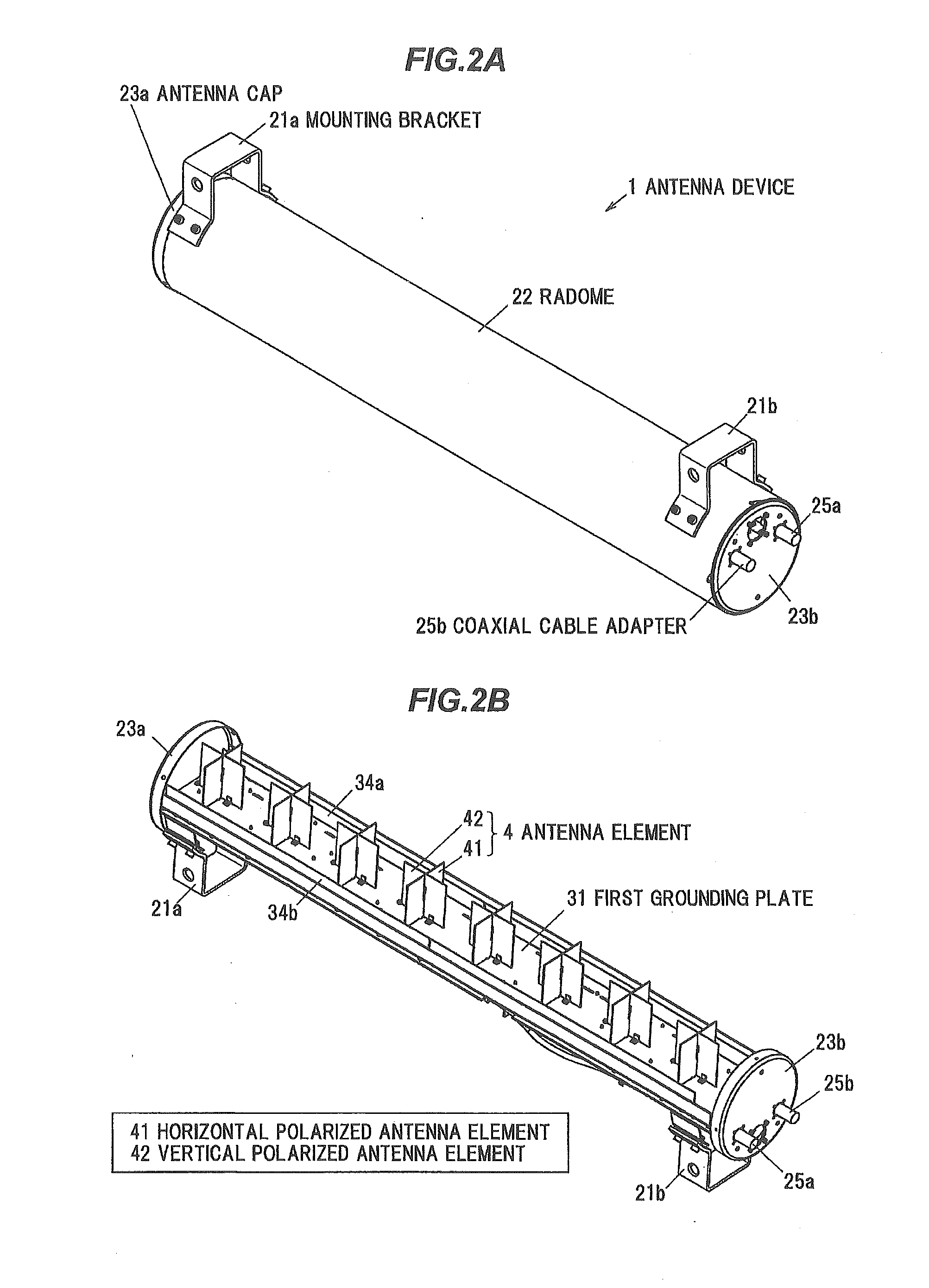
[0039]This antenna device 1 is used as a mobile phone base station antenna device, for example, and is configured as including a high frequency signal transmitting or receiving terminal 10, a distributor the triplate line 11, a dielectric phase shifter the triplate line 12, a feed line the triplate line 13, and an antenna element array 14 with a plurality of antenna elements arranged in an array.

[0040]When excitation power depending on a high frequency transmission signal is input to the high frequency signal transmitting or receiving terminal 10, the excitation power is distributed by the distributor the triplate line 11. The excitation power distributed is imparted with a specified amount of phase shift by the respective corresponding the dielectric phase shifter the triplate line 12, and is input to the respective corresponding feed line the...


PUM


Abstract

An antenna device includes an antenna element including a dielectric substrate including a first principal surface and a second principal surface, a built-in feed line provided on the first principal surface of the dielectric substrate, and a radiating element provided on the second principal surface of the dielectric substrate and along the built-in feed line so that the radiating element is fed from the built-in feed line, a triplate line including a first outer conductor and a second outer conductor parallel to each other, and a central conductor arranged therebetween to feed excitation power to the antenna element, a connecting member which electrically connects the central conductor and the built-in feed line, a projecting piece from one end of the dielectric substrate toward the second outer conductor, and a first hole and a second hole provided in the first outer conductor and in communication with each other. The first hole includes a first opposite surface to the connecting member with a specified space therebetween. The projecting piece is inserted in the second hole. The second hole includes an opposite regulating surface to the first principal surface of the projecting piece of the dielectric substrate, to regulate movement of the dielectric substrate toward the first opposite surface.

Description

[0001]The present application is based on Japanese patent application No.2013-163954 filed on Aug. 7, 2013, the entire contents of which are incorporated herein by reference.BACKGROUND OF THE INVENTION[0002]1. Field of the Invention[0003]This invention relates to an antenna device, which includes a triplate line capable of feeding high frequency signal dependent excitation power to a plurality of antenna elements.[0004]2. Description of the Related Art[0005]As a conventional antenna device, a cross dipole antenna device has been known, which is configured as one pair of dielectric substrates combined together. Refer to JP-A-2009-124403, for example.[0006]The antenna device described in JP-A-2009-124403 includes first and second rectangular dielectric substrates formed with a built-in feed line and a radiating element, and a square mount with the first and second dielectric substrates thereon. The first and second rectangular dielectric substrates are mounted in such a manner as to c...

Claims


Application Information

Patent Timeline
Patent Type & Authority Applications(United States)
IPC IPC(8): H01Q9/28
CPCH01Q9/285H01Q1/246H01Q21/08H01Q21/24
Inventor KITANO, NOBUAKIOGAWA, TOMOYUKIISO, NAOKIISHIGAMI, YOSHIAKI
Owner HITACHI METALS LTD
Why Eureka
Try Eureka