Seamless display manufacturing method

a liquid crystal display and manufacturing method technology, applied in the manufacture of electrode systems, electric discharge tubes/lamps, instruments, etc., can solve the problems of high production cost, low production yield, and inability to meet the requirements of large-scale panel development and manufacturing by various panel manufacturers, so as to maintain luminance uniformity

Active Publication Date: 2008-06-05
HU CHUNG MING
View PDF4 Cites 12 Cited by
  • Summary
  • Abstract
  • Description
  • Claims
  • Application Information

AI Technical Summary

Benefits of technology

[0010]In view of the restrictions and shortcomings of the liquid crystal display (LCD) image display of the prior art, the objective of the present invention is to disclose a manufacturing method of a seamless display, so that the image signal emitted from LC panel may incident upon and enter into the eyes of a viewer in a direction approximately perpendicular to the protection layer of LC panel, thus avoiding mixing of signals coming from the gaps in an assembled LC panel; meanwhile, the luminance of the image emitted from and near the gaps is enabled to be close to that of the central portion of the various panels assembled, thus creating and maintaining luminance uniformity for various portions in the assembled panel, and achieving the effect and objective of visually seamless image display.

Problems solved by technology

However, presently, the development and manufacturing of large-sized panel by the various panel manufacturers is still subject to the restrictions in cost and technology that has yet to be overcome.
Namely, for the large-sized panel, the production cost is high, yet its production yield is rather low, and this constitutes a great obstacle to the feasibility of its mass production.
However, in assembling a plurality of liquid crystal panels into a larger-sized one, the gaps in the assembled panel formed by side edges around the perimeter of a constituting unitary panel tend to cause the assembled large-sized panel to produce partitioned, discontinuous image displaying result.
An ordinary TV wall is taken as an example, in this case, even though the image produced may present large-sized presentation through a combination of the screens of a plurality of TV sets, thus facilitating outdoors display or viewing, yet the completeness of screen is adversely affected by the evident gaps produced by the outer edge of a screen of each of the respective TV sets.
Similarly, in combining a plurality of panels into a single unitary large-sized panel, the outer edges of the respective panels form visible and evident gaps in an assembled panel, hereby resulting in the partition of screen, and the visually imperfect image presentation.
Yet in applying this approach, the light transmission guide is required to contain optical fiber or glass tube capable of reflecting the light, and that leads to the high production cost of the light transmission guide; meanwhile, the overall thickness of the assembled display is too much, thus it is inconvenient to assemble and transport.
In addition, there are the problems of luminance uniformity between the entire assembled panel and a single unitary panel, since the central portion of LC panel is sure to have higher luminance than that of the edge portion, thus, usually, optical correction film (or light filtering sheet) is utilized to filter the light coming from the central portion of panel having higher luminance, so that the luminance of central portion approaching that of the surrounding portion.
However, this approach would lead to the overall degradation of the luminance of LC panel, yet the luminance difference between adjacent panels may still exist.
Moreover, in case that the matching between light transmission guide and pixels of panel is not appropriate, or it is not able to achieve optimum matching due to mechanical tolerance, and that may cause color or gray level distortion in displaying images, thus resulting in deviations from the input signals of the original panel.

Method used


Image

  • Seamless display manufacturing method
  • Seamless display manufacturing method
  • Seamless display manufacturing method

Examples


Embodiment Construction

[0046]The purpose, construction, features, and functions of the present invention can be appreciated and understood more thoroughly through the following detailed description with reference to the attached drawings.

[0047]Although, in the following, the preferred embodiments of the present invention will be described with reference to the attached drawings. However, it should be appreciated that the contents of the present invention can be modified within its scope and spirit by people skilled in the art, while achieving the effectiveness of the present invention. Therefore, the following description is a broad disclosure in general, and it is not intended to restrict the scope of the present invention.

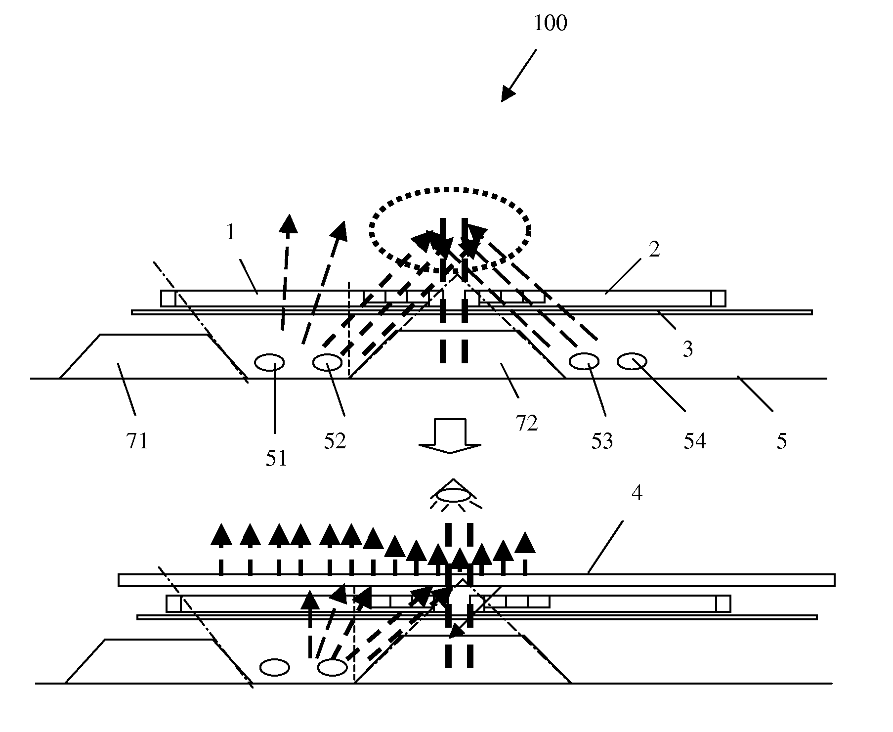
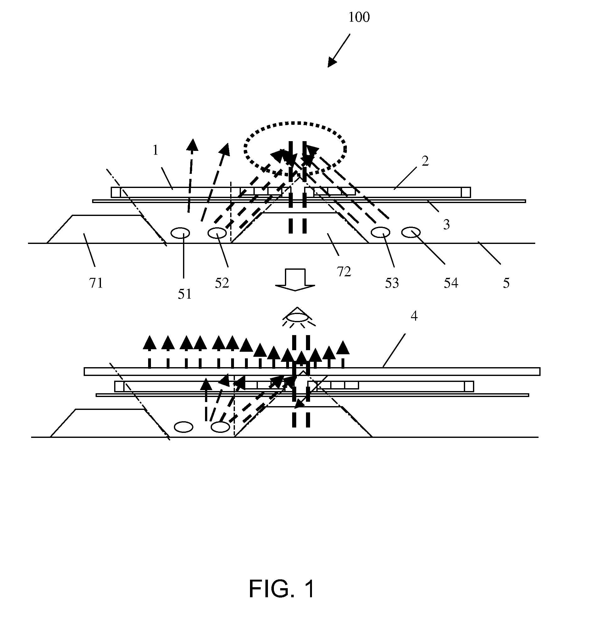
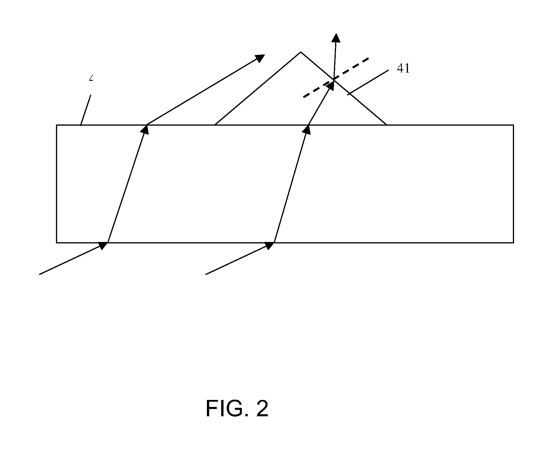
[0048]Firstly, please refer to FIG. 1, which is a schematic diagram of a structure of seamless display and the proceeding of an image displaying light according to the present invention. As shown in FIG. 1, display 100 includes a liquid crystal panel 1 and a liquid crystal panel 2, and...


PUM

PropertyMeasurementUnit
angleaaaaaaaaaa
micro-structuresaaaaaaaaaa
micro-structureaaaaaaaaaa

Abstract

Disclosed is a seamless display manufacturing method, comprising the following steps: fixing a light emitting source in a backlight module; fixing an optical film on the light emitting source; placing a partitioned structure on the optical film; aligning or overlapping the side edges of main bodies of adjacent liquid crystal panels, and putting them over the partitioned structure; and providing a protection layer having a micro-structure over a main body of a liquid crystal panel, thus forming an LCD display. Wherein, more than one LCD displays can be assembled to form an assembled LCD. The present invention also relates to a seamless display, comprising: a backlight module, that includes a plurality of light emitting sources; an optical film; a partitioned structure; a plurality of LCD panel main bodies; a protection layer having a micro-structure; and a locking portion, hereby forming a display unit. Wherein, the main bodies of a plurality of liquid crystal panels are put together through aligning or overlapping their respective side edges, and then are covered over the partitioned structure. The disclosure can be applied to form seamless large-sized image displaying panel, thus achieving the reduction of gap size between panel side edges in a large assembled panel and high quality image display.

Description

BACKGROUND OF THE INVENTION[0001]1. Field of the Invention[0002]The present invention relates to a method of manufacturing assembled liquid crystal display, that can be utilized in seamless image displaying large-sized panel.[0003]2. The Prior Arts[0004]Currently, due to the remarkable benefit and performance of liquid crystal panel in commercial advertisement and video entertainment, large-sized panel has become very popular and has a very good prospect and market potential. However, presently, the development and manufacturing of large-sized panel by the various panel manufacturers is still subject to the restrictions in cost and technology that has yet to be overcome. Namely, for the large-sized panel, the production cost is high, yet its production yield is rather low, and this constitutes a great obstacle to the feasibility of its mass production. Due to this reason, the design and manufacturing of large-sized panel by assembling and making use of the panels of currently availa...

Claims


Application Information

Patent Timeline
Patent Type & Authority Applications(United States)
IPC IPC(8): G02F1/1335H01J9/24
CPCG02F1/13336G02F1/133504G02F1/133605H01J61/307H01J9/205H01J9/241H01J61/305G02F1/133606G02F1/1333
Inventor HU, CHUNG-MING
Owner HU CHUNG MING
Why Eureka
Try Eureka