Plasma display panel and plasma display device

Inactive Publication Date: 2006-07-27
FUJITSU HITACHI PLASMA DISPLAY LTD
View PDF5 Cites 0 Cited by
  • Summary
  • Abstract
  • Description
  • Claims
  • Application Information

AI Technical Summary

Benefits of technology

[0029] As described above, if the third electrode is operated so as to generate a trigger discharge and not to be related to the main

Problems solved by technology

Therefore, the intensity of the sustain discharge for each cell is varied depending

Method used


Image

  • Plasma display panel and plasma display device
  • Plasma display panel and plasma display device
  • Plasma display panel and plasma display device

Examples


first embodiment

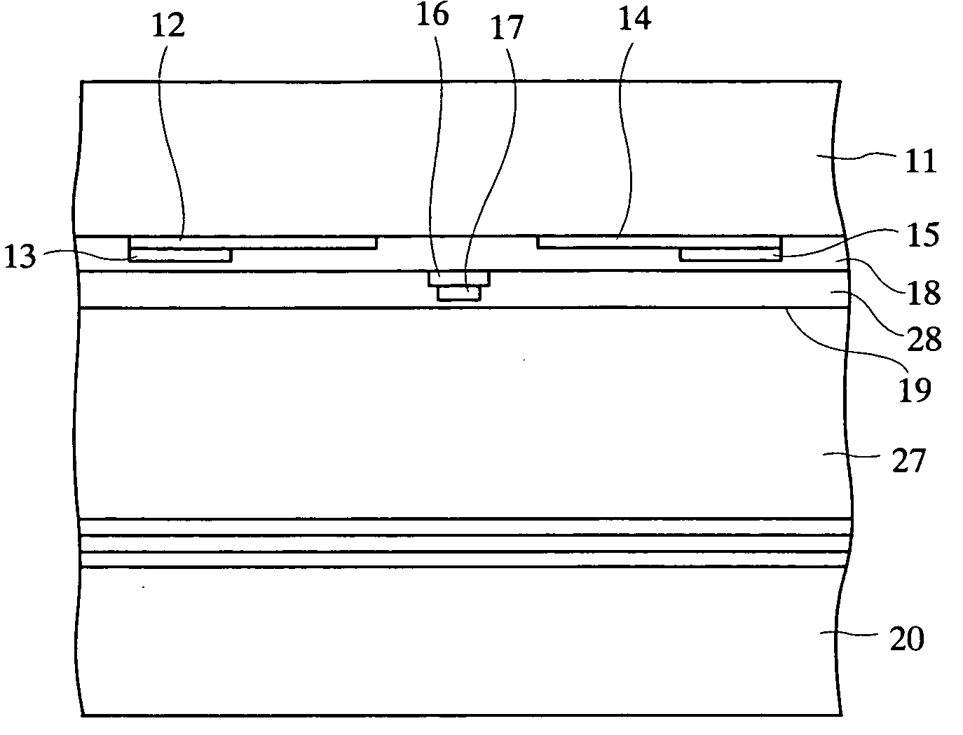
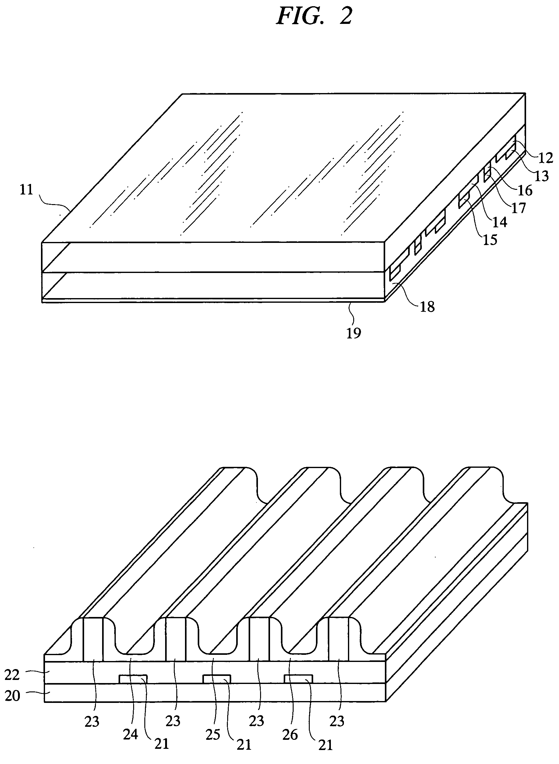
[0071]FIG. 2 is an exploded perspective view of the PDP of the As shown in FIG. 2, on a front (first) glass substrate 11, laterally extending first (X) bus electrodes 13 and second (Y) bus electrodes 15 are alternately disposed in parallel to each other so as to form pairs. X and Y optically transparent electrodes (discharge electrodes) 12 and 14 are provided so as to be overlapped over the X and Y bus electrodes 13 and 15, and parts of the X and Y discharge electrodes 12 and 14 are extending toward the side of the opposing electrodes. A third (Z) discharge electrode 16 and a third (Z) bus electrode 17 overlapped with each other are provided between the X and Y bus electrodes 13 and 15 of each pair. For example, the bus electrodes 13, 15, and 17 are formed of metal layers and the discharge electrodes 12, 14, and 16 are formed of ITO films or the like, and the resistance values of the bus electrodes 13, 15, and 17 are lower than or equal to the resistance values of the discharge ele...

second embodiment

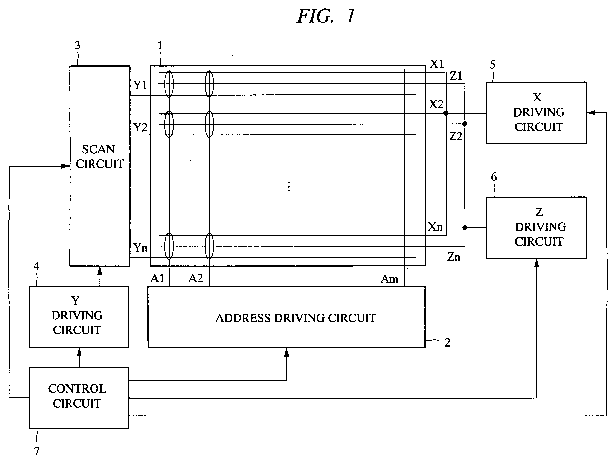
[0114] As shown in FIG. 13, the PDP device of the second embodiment has the address driving circuit 2 which drives the address electrodes, the scanning circuit 3 which applies scan pulses to the Y electrodes, an odd-number Y driving circuit 41 which applies voltages other than the scan pulse to the odd-numbered Y electrodes in common via the scanning circuit 3, an even-number Y driving circuit 42 which applies voltages other than the scan pulse to the even-numbered Y electrodes in common via the scanning circuit 3, an odd-number X driving circuit 51 which applies voltages to the odd-numbered X electrodes in common, an even-number X driving circuit 52 which applies voltages to the even-numbered X electrodes in common, a first Z driving circuit 61 which drives the Z electrodes of the first group in common, a second Z driving circuit 62 which drives the Z electrodes of the second group in common, a third Z driving circuit 63 which drives the Z electrodes of the third group in common, a...


PUM


Abstract

A plasma display panel capable of reducing a peak value of a sustain discharge current without generating luminance nonuniformity is provided. The plasma display panel comprises: a plurality of first, second, and third electrodes disposed to be adjacent to each other and extending in a first direction, the third electrodes being provided between the first electrodes and the second electrodes where the discharge is repeated; and a dielectric layer covering the electrodes, wherein the space between the first electrode and the second electrode is approximately constant over an entire display area width of the panel, and a space between the third electrode and the first and second electrodes is varied depending on positions in the entire display area width of the panel in a first direction.

Description

CROSS-REFERENCE TO RELATED APPLICATION [0001] The present application claims priority from Japanese Patent Application No. JP 2005-15156 filed on Jan. 24, 2005, the content of which is hereby incorporated by reference into this application. TECHNICAL FIELD OF THE INVENTION [0002] The present invention relates to an A / C plasma display panel (PDP) and a plasma display device (PDP device) used for a display device of a personal computer and a workstation, a flat TV, and a plasma display for displaying advertisements, information, and others. BACKGROUND OF THE INVENTION [0003] In AC color PDP devices, an address / display separation (ADS) method in which a period when the cells to be displayed are determined (address period) and a display period when discharges for display lighting are performed (sustain period) are separated is widely employed. In this method, charge is accumulated in the cells, which are to be turned on, in the address period, and discharges for display are performed by...

Claims


Application Information

Patent Timeline
IPC IPC(8): G09G3/10G09F9/30G09G3/20G09G3/288G09G3/291G09G3/292G09G3/293G09G3/294G09G3/298G09G3/299H01J11/12H01J11/22H01J11/24H01J11/26H01J11/28H01J11/32H01J11/34
CPCG09G3/2942G09G3/2986H01J11/12H01J11/28H01J2211/323
Inventor KOBAYASHI, TAKAYUKISASAKI, TAKASHIITOKAWA, NAOKITERAOKA, TORU
Owner FUJITSU HITACHI PLASMA DISPLAY LTD
Why Eureka
Try Eureka