Elastic wave device and method for manufacturing the same

a technology of elastic wave and thin film, applied in the direction of impedence network, electric apparatus, etc., can solve the problems of affecting the performance of the device, the energy of the surface acoustic wave device is leaking, and the propagation loss is considered. , to achieve the effect of restoring piezoelectricity, good characteristics, and strengthening bonding

Active Publication Date: 2013-10-31
MURATA MFG CO LTD
View PDF7 Cites 132 Cited by
  • Summary
  • Abstract
  • Description
  • Claims
  • Application Information

AI Technical Summary

Benefits of technology

[0030]In another specific aspect of the method for manufacturing an elastic wave device according to a preferred embodiment of the present invention, the method further includes a step of, after separating the remaining portion of the piezoelectric substrate, heating the piezoelectric film disposed on the low-acoustic-velocity film to recover piezoelectricity. In such a case, since the piezoelectricity of the piezoelectric film can be recovered by heating, it is possible to provide an elastic wave device having good characteristics.
[0031]In another specific aspect of the method for manufacturing an elastic wave device according to a preferred embodiment of the present invention, the method further includes a step of, prior to bonding the supporting substrate, performing mirror finishing on the surface of

Problems solved by technology

However, there is considerable propagation loss, and surface acoustic waves cannot be effectively confined within the piezoelectric thin film.
Consequently, the

Method used


Image

  • Elastic wave device and method for manufacturing the same
  • Elastic wave device and method for manufacturing the same
  • Elastic wave device and method for manufacturing the same

Examples


second preferred embodiment

[0102]Characteristics of a surface acoustic wave device according to a second preferred embodiment having the structure described below were simulated by a finite element method. The electrode structure was the same as that shown in FIG. 1B.

[0103]An IDT electrode was an Al film with a thickness of 0.08λ. A piezoelectric film was composed of 38.5° Y cut LiTaO3 film, and the thickness thereof was in a range of 0 to 3λ. A low-acoustic-velocity film was composed of silicon oxide, and the thickness thereof was 0 to 2λ. A high-acoustic-velocity film was composed of aluminum oxide, and the thickness thereof was 1.5λ. A supporting substrate was composed of alumina.

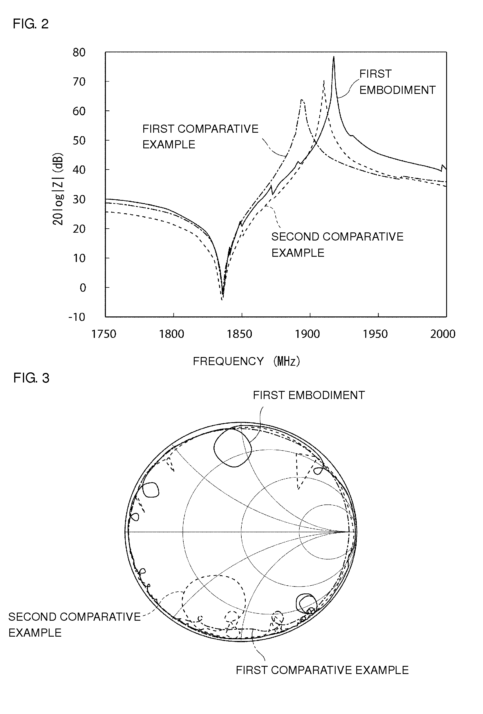
[0104]The results are shown in FIGS. 7 to 10.

[0105]FIG. 7 is a graph showing the relationship between the LiTaO3 film thickness, the acoustic velocity of the U2 mode which is the usage mode, and the normalized film thickness of the silicon oxide film. Furthermore, FIG. 8 is a graph showing the relationship between the LiTaO3 film ...

third preferred embodiment

[0126]As a third preferred embodiment, surface acoustic wave devices same as those of the first preferred embodiment were fabricated. The materials and thickness were as described below.

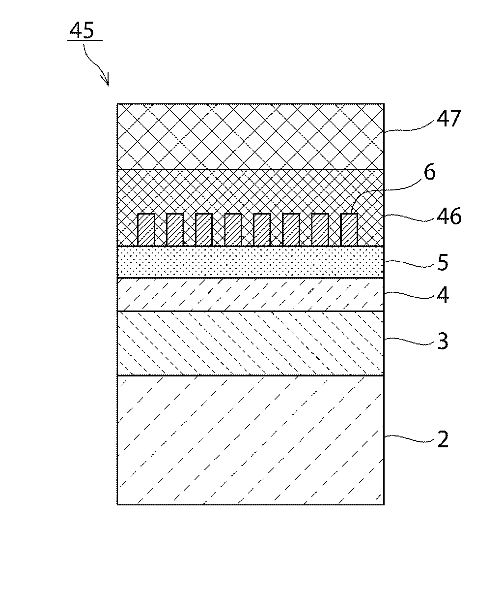
[0127]A laminated structure included an Al film with a thickness of 0.08λ as an IDT electrode 6 / a LiTaO3 film with a thickness of 0.25λ as a piezoelectric film 4 / a silicon oxide film with a thickness in the range of 0 to 2λ as a low-acoustic-velocity film 4 / a high-acoustic-velocity film. As the high-acoustic-velocity film, a silicon nitride film, an aluminum oxide film, or diamond was used. The thickness of the high-acoustic-velocity film 3 was 1.5λ.

[0128]FIGS. 15 and 16 are graphs showing the relationship between the thickness of the silicon oxide film and the acoustic velocity and the relationship between the thickness of the silicon oxide film and the electromechanical coupling coefficient k2, respectively, in the third preferred embodiment.

[0129]The acoustic velocity of the bulk wave (S wave) in ...

fourth preferred embodiment

[0132]In a fourth preferred embodiment, while changing the Euler angles (0°, θ, ψ) of the piezoelectric film, the electromechanical coupling coefficient of a surface acoustic wave containing as a major component the U2 component (SH component) was measured.

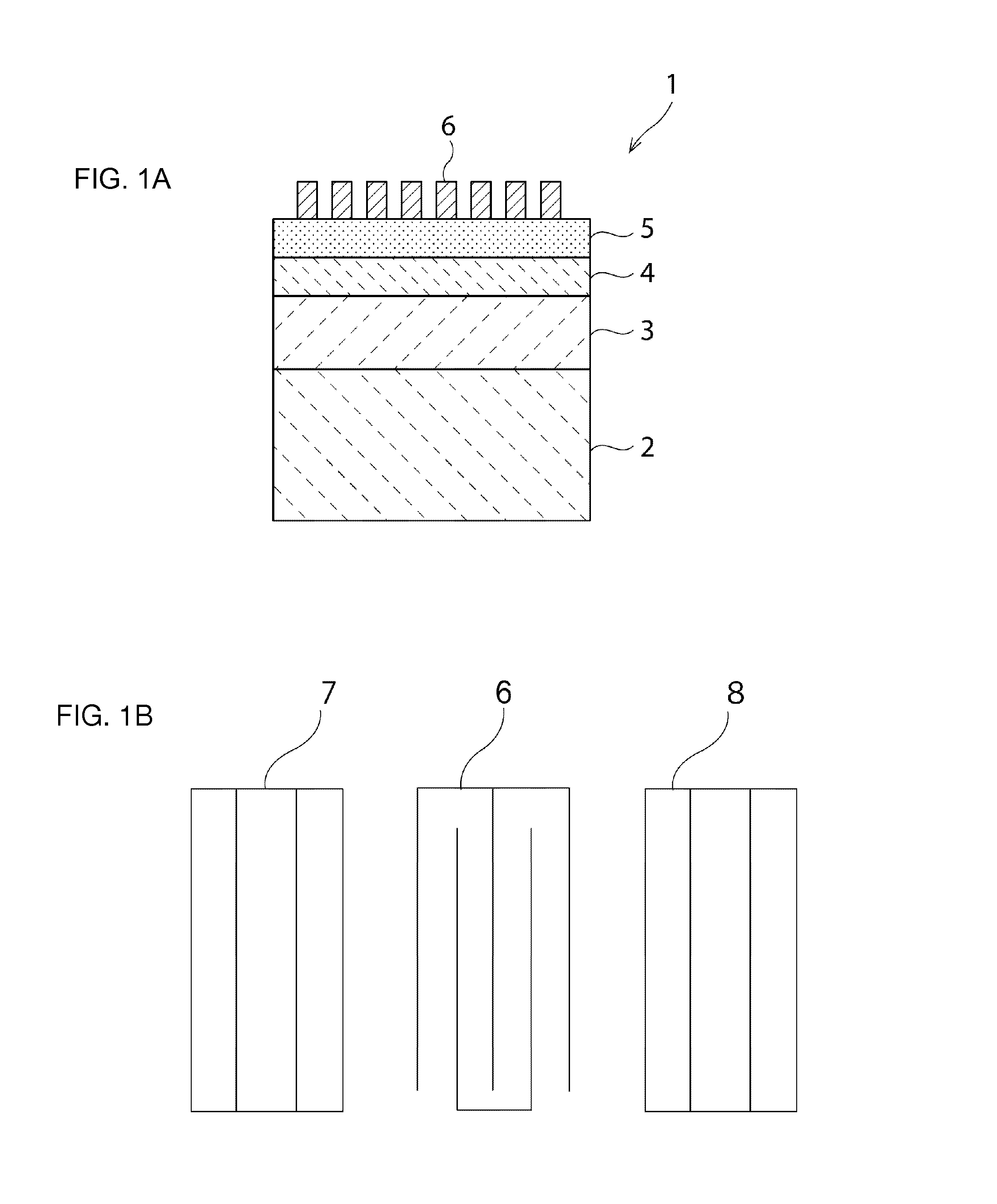
[0133]A laminated structure was composed of IDT electrode 6 / piezoelectric film 5 / low-acoustic-velocity film 4 / high-acoustic-velocity film 3 / supporting substrate 2. As the IDT electrode 6, Al with a thickness of 0.08λ was used. As the piezoelectric film, LiTaO3 with a thickness of 0.25λ was used. As the low-acoustic-velocity film 4, silicon oxide with a thickness of 0.35λ was used. As the high-acoustic-velocity film 3, an aluminum nitride film with a thickness of 1.5λ was used. As the supporting substrate 2, glass was used.

[0134]In the structure described above, regarding many surface acoustic wave devices with Euler angles (0°, θ, ψ) in which θ and ψ were varied, the electromechanical coupling coefficient was obtained by FEM. As a...


PUM

PropertyMeasurementUnit
Angleaaaaaaaaaa
Thicknessaaaaaaaaaa
Piezoelectricityaaaaaaaaaa

Abstract

An elastic wave device includes a supporting substrate, a high-acoustic-velocity film stacked on the supporting substrate and in which an acoustic velocity of a bulk wave propagating therein is higher than an acoustic velocity of an elastic wave propagating in a piezoelectric film, a low-acoustic-velocity film stacked on the high-acoustic-velocity film and in which an acoustic velocity of a bulk wave propagating therein is lower than an acoustic velocity of a bulk wave propagating in the piezoelectric film, the piezoelectric film is stacked on the low-acoustic-velocity film, and an IDT electrode stacked on a surface of the piezoelectric film.

Description

BACKGROUND OF THE INVENTION[0001]1. Field of the Invention[0002]The present invention relates to an elastic wave device preferably for use in a resonator, a bandpass filter, or the like and a method for manufacturing the same. More particularly, the present invention relates to an elastic wave device having a structure including a supporting substrate, a piezoelectric layer, and a layer of another material disposed therebetween, and a method for manufacturing the same.[0003]2. Description of the Related Art[0004]Elastic wave devices have been widely used as resonators and bandpass filters, and in recent years, there has been a need for increasing the frequency thereof. Japanese Unexamined Patent Application Publication No. 2004-282232 described below discloses a surface acoustic wave device in which a hard dielectric layer, a piezoelectric film, and an IDT electrode are stacked in that order on a dielectric substrate. In such a surface acoustic wave device, by disposing the hard die...

Claims


Application Information

Patent Timeline
IPC IPC(8): H03H9/54
CPCH03H9/54H03H3/10H03H9/0222H03H9/02574H03H9/02834Y10T29/42Y10T29/49155Y10T29/49005H03H3/08H03H9/145H03H9/25H03H3/02H03H2003/023H03H3/04H03H2003/027H10N30/01H10N30/80H10N30/85H10N30/87H10N30/877
Inventor WATANABE, MUNEHISAIWAMOTO, HIDEKIKANDO, HAJIMEKIDO, SYUNSUKE
Owner MURATA MFG CO LTD
Why Eureka
Try Eureka