Coordinated-design supporting apparatus, coordinated-design supporting method, computer product, and printed-circuit-board manufacturing method

a technology of supporting apparatus and coordinated design, which is applied in the direction of cad circuit design, program control, instruments, etc., can solve the problem that the packaging designer cannot consider the pin assignmen

Inactive Publication Date: 2008-06-05
FUJITSU LTD
View PDF25 Cites 15 Cited by
  • Summary
  • Abstract
  • Description
  • Claims
  • Application Information

AI Technical Summary

Benefits of technology

[0010]According to another aspect of the present invention, a method for supporting coordinated-design includes receiving pin assignment information that is created by using a PLD-designing CAD with respect to a PLD; and creating a temporary component shape type library as a temporary library subject to the PLD by using the pin assignment information, the temporary component shape type library being alternative to a component shape type library required by a package-designing CAD apparatus.

Problems solved by technology

However, there is a problem that a component shape type library is required to consider a package design by using the package-designing CAD apparatus, though, there is no component shape type library of the PLD component when the PLD designer and the package designer consider an early pin assignment.
Therefore, the package designer cannot consider the pin assignment by using the package-designing CAD apparatus.

Method used


Image

  • Coordinated-design supporting apparatus, coordinated-design supporting method, computer product, and printed-circuit-board manufacturing method
  • Coordinated-design supporting apparatus, coordinated-design supporting method, computer product, and printed-circuit-board manufacturing method
  • Coordinated-design supporting apparatus, coordinated-design supporting method, computer product, and printed-circuit-board manufacturing method

Examples


first embodiment

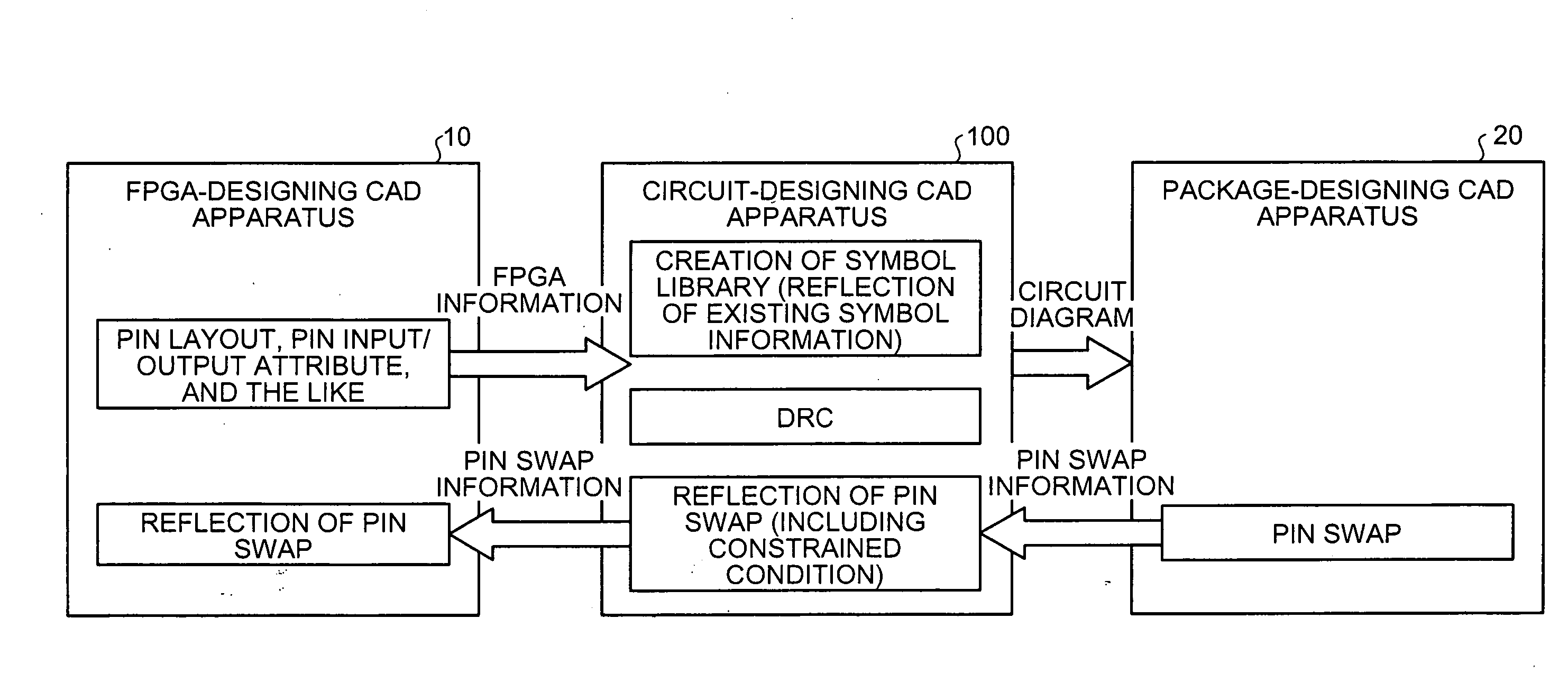
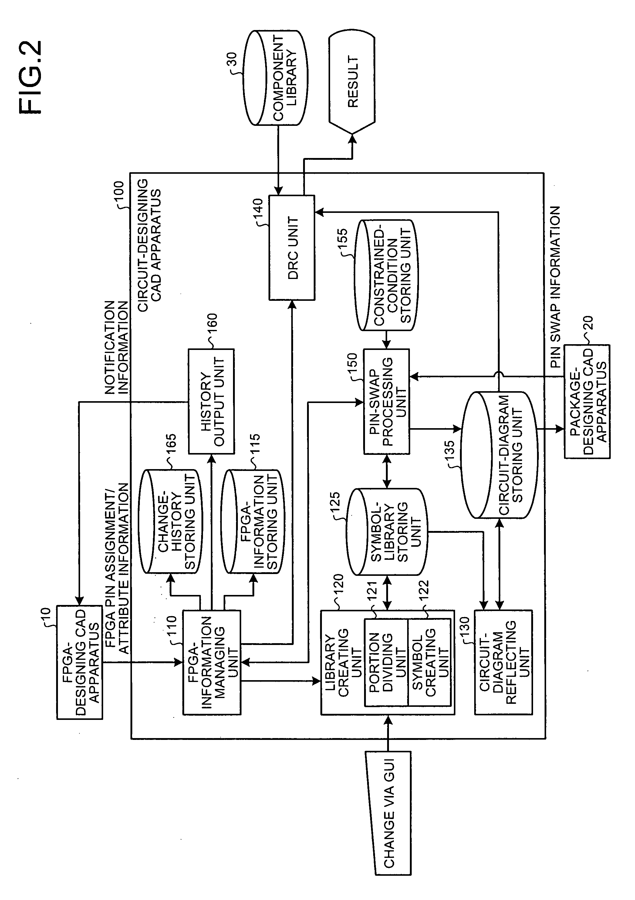
[0110]As described above, in the first embodiment, the FPGA-information managing unit 110 included in the circuit-designing CAD apparatus 100 retrieves FPGA information, such as pin assignment information and attribute information, which is created by the FPGA-designing CAD apparatus 10, and the library creating unit 120 creates a symbol library by using the FPGA information. Therefore, the circuit designer needs not create the symbol library of the FPGA, and thus it is possible to reduce workloads on the circuit designer.

[0111]Furthermore, at the time of creating a symbol library, if an FPGA subjected to create a symbol library is arranged in the circuit diagram, the library creating unit 120 manages not to change a portion assignment and a pin layout of the existing symbol library arranged in the circuit diagram as much as possible. Also, when the circuit-diagram reflecting unit 130 arranges a symbol of an FPGA that a symbol library is newly created in the circuit diagram, the sym...

second embodiment

[0118]In this manner, in the second embodiment, the temporary-library creating apparatus 200 receives the FPGA pin information that is created by the FPGA-designing CAD apparatus 10, and creates a temporary component shape type library with respect to the FPGA. Thus, it is possible to consider a pin assignment by using the package-designing CAD apparatus 20.

[0119]Subsequently, a configuration of the FPGA coordinated design system according to the second embodiment is explained. FIG. 20 is a functional block diagram of the configuration of the FPGA coordinated design system according to the second embodiment. As shown in the drawing, the FPGA coordinated design system includes the FPGA-designing CAD apparatus 10, the package-designing CAD apparatus 20, and the temporary-library creating apparatus 200. The temporary-library creating apparatus 200 includes a net-list retrieving unit 210, a net-list managing unit 220, a net-list converting unit 230, an FPGA-design-CAD interface unit 240...


PUM


Abstract

An FPGA-design-CAD interface unit retrieves pin assignment information created by an FPGA-designing CAD apparatus. An FPGA-pin-information managing unit manages the pin assignment information as FPGA pin information. A temporary-library creating unit creates a temporary component shape type library by using the FPGA pin information and outputs the temporary component shape type library in a form capable of being read by a package-designing CAD apparatus to a file.

Description

BACKGROUND OF THE INVENTION[0001]1. Field of the Invention[0002]The present invention relates to a technology that enables consideration of an early pin assignment by using a package-designing CAD apparatus in designing a printed circuit board including a PLD component.[0003]2. Description of the Related Art[0004]In designing a printed circuit board including a PLD component such as Field Programmable Gate Array (FPGA), a PLD designer, a circuit designer, and a package designer exchange design information such as pin assignment information.[0005]A PLD-designing CAD apparatus for supporting PLD designing, a circuit-designing CAD apparatus for supporting circuit designing, and a package-designing CAD apparatus for supporting package designing respectively hold design information, and thus it is important to maintain a consistency among the design information held by each of the apparatuses. Therefore, for example, when pin assignment is changed in package designing, the change needs t...

Claims


Application Information

Patent Timeline
Patent Type & Authority Applications(United States)
IPC IPC(8): G06F17/50
CPCG06F17/5054G06F30/34
Inventor KATO, YOSHIYUKIAOYAMA, HISASHI
Owner FUJITSU LTD
Why Eureka
Try Eureka