Multi-chip package structure and method of forming the same

a multi-chip and package technology, applied in the field of semiconductor packaging, can solve the problems of reducing the yield, reducing the yield, and the frame package technology is already not suitable for advanced semiconductor dies, and achieve the effect of raising the yield of the package structur

Inactive Publication Date: 2008-06-12
ADVANCED CHIP ENG TECH
View PDF3 Cites 191 Cited by
  • Summary
  • Abstract
  • Description
  • Claims
  • Application Information

AI Technical Summary

Benefits of technology

[0013]Still another objective of the present invention is to avoid problems of signal coupling and signal interface.
[0014]Still another objective of the present invention is to raise the yield of the package structure.

Problems solved by technology

It causes the packaging for the semiconductor dies to become more difficult and decrease the yield.
The earlier lead frame package technology is already not suitable for the advanced semiconductor dies due to the density of the pins thereof is too high.
As aforementioned, the size of the package is limited by the chip size, and the I / O pads are contacted through wire bonding in the conventional arts.
Therefore, the package size is incapable of extension and a too short pitch among via results in a problem of signal coupling or signal interface, poor heat dissipation performance.

Method used


Image

  • Multi-chip package structure and method of forming the same
  • Multi-chip package structure and method of forming the same
  • Multi-chip package structure and method of forming the same

Examples


Embodiment Construction

[0029]Some sample embodiments of the invention will now be described in greater detail. Nevertheless, it should be recognized that the present invention can be practiced in a wide range of other embodiments besides those explicitly described, and the scope of the present invention is expressly not limited expect as specified in the accompanying claims.

[0030]Then, the components of the different elements are not shown to scale. Some dimensions of the related components are exaggerated and meaningless portions are not drawn to provide a more clear description and comprehension of the present invention.

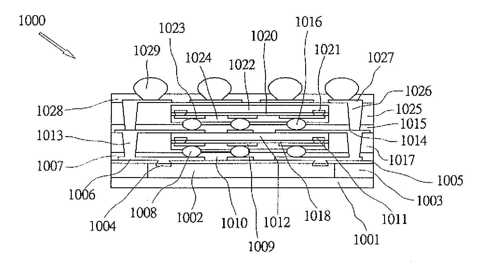
[0031]The essence of the present invention is to disclose package in package (PIP) structure which is capable of obtaining an appropriate package size by adjusting distance between via through holes. Therefore, the package structure has an adjustable size of package due to die mounted on a substrate. Moreover, the die may be packaged with passive components (ex. capacitors) or other dies...


PUM


Abstract

To pick and place standard first chip size package on a base with a second chip for obtaining an appropriate stacking chip size package than the original chip size package. The package structure has a larger chip size package than the size of the traditional stacking package. Moreover, the terminal pins of the flip chip package may be located on peripheral of LGA package or on array of BGA package.

Description

BACKGROUND OF THE INVENTION [0001]1. Field of the Invention[0002]This invention relates to a package for semiconductors, and more particularly to a multi-chip package and method of the same.[0003]2. Description of the Prior Art[0004]The semiconductor technologies are developing very fast, and especially semiconductor dies have a tendency toward miniaturization. However, the requirements for the functions of the semiconductor dies have an opposite tendency to variety. Namely, the semiconductor dies must have more I / O pads into a smaller area, so the density of the pins is raised quickly. It causes the packaging for the semiconductor dies to become more difficult and decrease the yield.[0005]The main purpose of the package structure is to protect the dies from outside damages. Furthermore, the heat generated by the dies must be diffused efficiently through the package structure to ensure the operation the dies.[0006]The earlier lead frame package technology is already not suitable for...

Claims


Application Information

Patent Timeline
Patent Type & Authority Applications(United States)
IPC IPC(8): H01L23/488H01L21/56
CPCH01L24/96H01L24/18H01L25/0657H01L25/50H01L2224/16H01L2224/48091H01L2225/06513H01L2225/06524H01L2225/06586H01L2924/01013H01L2924/01015H01L2924/01027H01L2924/01029H01L2924/01033H01L2924/01047H01L2924/01074H01L2924/01075H01L2924/01078H01L2924/01079H01L2924/01082H01L2924/09701H01L2924/19041H01L2924/19043H01L24/97H01L2224/0401H01L2924/18161H01L2924/15311H01L2924/01005H01L2924/01006H01L2924/01068H01L2924/10253H01L2224/04105H01L2224/12105H01L2224/32225H01L2224/73267H01L2924/00014H01L2924/00H01L24/19H01L24/20H01L2224/16145H01L2224/24226H01L2224/24246H01L2224/32245H01L2224/73209H01L2224/97H01L2924/181H01L2224/83H01L2224/82H01L2224/81H01L2924/00012H01L23/12H01L23/48
Inventor YANG, WEN-KUNYU, CHUN-HUICHOU, CHAO-NANLIN, CHIH-WEIHUANG, CHING-SHUN
Owner ADVANCED CHIP ENG TECH
Why Eureka
Try Eureka