Semiconductor memory device capable of easily performing delay locking operation under high frequency system clock

a memory device and semiconductor technology, applied in the direction of digital storage, pulse automatic control, generating/distributing signals, etc., can solve the problem of difficulty in performing exact delay locking operation

Active Publication Date: 2008-06-12
SK HYNIX INC
View PDF7 Cites 46 Cited by
  • Summary
  • Abstract
  • Description
  • Claims
  • Application Information

AI Technical Summary

Benefits of technology

[0014]In accordance with an aspect of the present invention, there is provided a semiconductor memory device comprising: a first clock buffer for outputting a first internal clock signal by buffering a system clock signal in response to an inverted signal of the system clock signal and for correcting a duty cycle ratio of the first internal clock signal in response to a control signal; a second clock buffer for outputting a second internal clock signal by buffering the inverted signal of the system clock signal in response to the system clock signal and for correcting a duty cycle ratio of the second internal clock signal in response to the control signal; an analog duty cycle correction circuit for outputting the control signal corresponding to the duty cycle ratio of the first and second internal clock signals; a mixing circuit for mixing the first and second internal clock signals and for outputting a third internal clock signal whose duty cycle is corrected; and a DLL circuit for outputting a delay-locked clock signal by using the third internal clock signal.
[0015]In accordance with another aspect of the present invention, there is provided a semiconductor memory device comprising: a first clock buffer for outputting a first internal clock signal by buffering a system clock signal in response to an inverted signal of the system clock signal and for correcting a duty cycle ratio of the first internal clock signal in response to a control signal; a second clock buffer for outputting a second internal clock signal by buffering the inverted signal of the system clock signal in response to the system clock signal and for correcting a duty cycle ratio of the second internal clock signal in response to the control signal; an analog duty cycle correction circuit for outputting the control signal corresponding to the duty cycle ratio of the first and second internal clock signals; a mixing circuit for mixing the first and second internal clock signals and for outputting a third internal clock signal whose duty cycle is corrected; a first DLL circuit for performing a delay locking operation based on a rising edge of the third internal clock and a first divided clock signal; a detecting unit for activating and outputting a detecting signal when a section between the rising and a falling edges of the third internal clock signal is smaller than a stored value; a first dividing circuit for outputting the first divided clock signal to the first DLL circuit in response to the detecting signal, wherein the first divided clock signal is produced by dividing an output of the first DLL circuit; a second DLL circuit for performing a delay locking operation based on the falling edge of the third internal clock signal and a second divided clock signal; and a second dividing circuit for outputting the second divided clock signal to the second DLL circuit in response to the detecting signal, wherein the second divided clock signal is produced by dividing an output of the second DLL circuit.
[0016]In accordance with another aspect of the present invention, there is provided a method for driving a semiconductor memory device comprising the steps of: outputting a first internal clock signal by buffering a system clock signal in response to an inverted system clock signal, wherein the first internal clock signal is outputted with a duty cycle correction in response to a control signal; outputting a second internal clock signal by buffering the inverted system clock signal in response to the system clock signal, wherein the second internal clock signal is outputted with a duty cycle correction in response to the control signal; outputting the control signal corresponding to a duty cycle ratio of the first and second internal clock signals; mixing the first and second internal clock signals for outputting a duty cycle-corrected third internal clock signal; and outputting a delay-looked clock signal by using the third internal clock signal.

Problems solved by technology

However, since the synchronous memory device is not sufficient to satisfy the required data input / output speed, a DDR (Double Data Rate) synchronous memory device, in which the data are inputted or outputted in synchronization with both a falling edge and a rising edge of the system clock signal, has been developed.
However, the system clock signal inputted to the memory device reaches the data output circuit with a delay time which is inevitably caused by a clock input buffer and a signal transmission line in the memory device.
Particularly, since the second DLL circuit 18B operates with the time difference of the half clock being different from the first DLL circuit 18A, it is very difficult to perform an exact delay locking operation.

Method used


Image

  • Semiconductor memory device capable of easily performing delay locking operation under high frequency system clock
  • Semiconductor memory device capable of easily performing delay locking operation under high frequency system clock
  • Semiconductor memory device capable of easily performing delay locking operation under high frequency system clock

Examples


Embodiment Construction

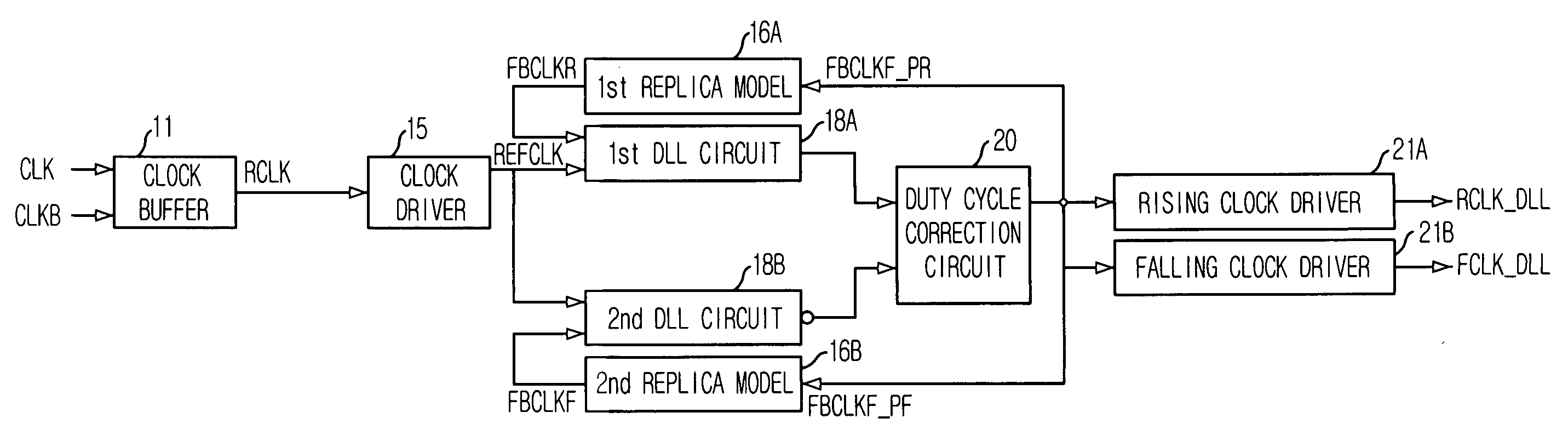
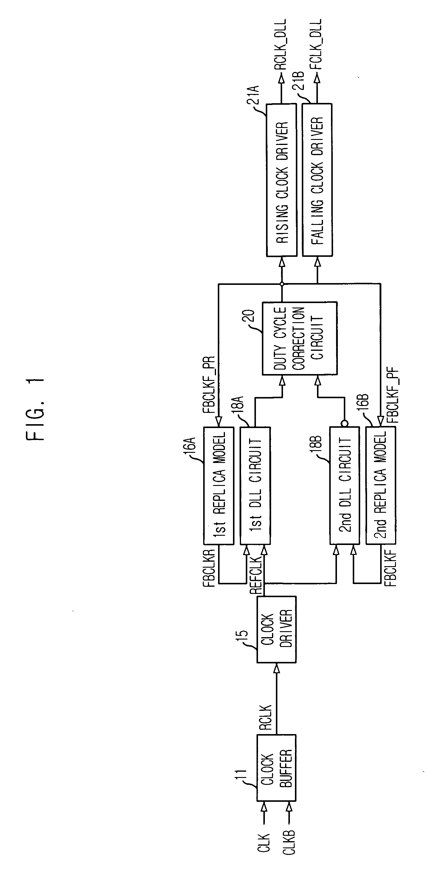
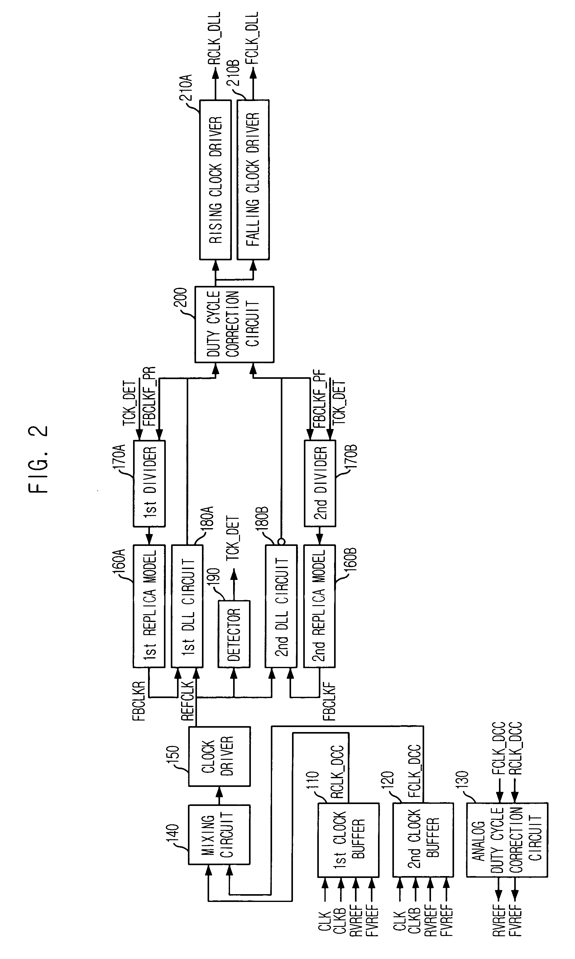
[0022]An object of the present invention is to provide a semiconductor memory device capable of easily performing a delay locking operation under a high frequency of system clock signal.

[0023]The semiconductor memory device according to the preferred embodiment of the present invention is characterized in that: first, an input unit to which the system clock signal is inputted performs the duty cycle correction and a DLL circuit receives the duty cycle corrected clock signal; second, the delay locking operation is performed after dividing the duty cycle corrected reference signal when the frequency of it is higher than a predetermined value; third, an output of the DLL circuit is directly used to make a feedback clock signal without the process of the duty cycle correction. The semiconductor memory device according to the present invention, with the above-described characteristics, can easily perform the delay locking operation using the system clock signal. The semiconductor memory ...


PUM


Abstract

A semiconductor memory device includes a first clock buffer for outputting a first internal clock signal in response to an inverted signal of the system clock signal and for correcting a duty cycle ratio of the first internal clock signal in response to a control signal; a second clock buffer for outputting a second internal clock signal in response to the system clock signal and for correcting a duty cycle ratio of the second internal clock signal in response to the control signal; an analog duty cycle correction circuit for outputting the control signal corresponding to the duty cycle ratio of the first and second internal clock signals; a mixing circuit for mixing the first and second internal clock signals and for outputting a third internal clock signal whose duty cycle is corrected; and a DLL circuit for outputting a delay-locked clock signal by using the third internal clock signal.

Description

CROSS-REFERENCE TO RELATED APPLICATIONS[0001]The present invention claims priority of Korean patent application no. 10-2006-0096481, filed in the Korean Patent Office on Sep. 29, 2006, which is incorporated by reference in its entirety.BACKGROUND OF THE INVENTION[0002]The present invention relates to a semiconductor memory device; and, more particularly, to a delay locked loop of the semiconductor memory device.[0003]In a system consisting of a plurality of semiconductor devices, a semiconductor memory device is used as an apparatus to store data. When data are required in a data processing unit, for example, the central processing unit (CPU) etc., the semiconductor memory device outputs data corresponding to an address signal which is inputted from an apparatus to demand the data, or stores the data in a location corresponding to the address signal provided from an apparatus.[0004]As the working speed of the system consisting of semiconductor devices becomes faster and the semicond...

Claims


Application Information

Patent Timeline
Patent Type & Authority Applications(United States)
IPC IPC(8): H03L7/00
CPCG06F1/04G11C7/22H03L7/0812H03K5/1565G11C7/222G11C7/1072G11C7/225G11C2207/2254
Inventor YOU, MIN-YOUNGLEE, SEONG-JUN
Owner SK HYNIX INC
Why Eureka
Try Eureka