Display device and drive method for same

a technology of a display device and a drive method, which is applied in the direction of electric digital data processing, instruments, computing, etc., can solve the problems of prone to variation in the threshold voltage, difficulty in enhancing the size and definition of the display device, and difficulty in identifying the characteristics, so as to prevent the decrease in the compensation accuracy and reduce the compensation accuracy. , the effect of preventing the number of times of characteristic detection

Active Publication Date: 2016-04-14
SHARP KK
View PDF3 Cites 37 Cited by
  • Summary
  • Abstract
  • Description
  • Claims
  • Application Information

AI Technical Summary

Benefits of technology

[0083]According to the first aspect of the present invention, the drive method for a display device having a pixel circuit including an electro-optical element (for example, an organic EL element) in which brightness is controlled by a current, and including a drive transistor for controlling a current to be supplied to the electro-optical element includes the noise measurement step of measuring noise. When the magnitude of the noise detected in the noise measurement step is less than the standard value, the video signal is corrected by using the correction data obtained in consideration of the detection result of the characteristics of the drive transistor and the electro-optical element. The video signal thus corrected is supplied to the pixel circuit, and accordingly, a drive current with such a magnitude that compensates for the deterioration of the drive transistor and the electro-optical element is supplied to the electro-optical element. Here, when the magnitude of the noise detected in the noise measurement step is the standard value or more, the correction data is not updated. That is to say, the correction data is not updated at such a time when an error to an unignorable extent occurs between the original current value and the measurement value with regard to the detection current for the external compensation for the deterioration of the circuit element. Hence, the decrease in the compensation accuracy, which is caused by a fact that the value of the correction data becomes an inappropriate value, is prevented. Thus, in the display device in which the external compensation technology for compensating for the deterioration of the circuit element is adopted, it becomes possible to prevent the decrease in the compensation accuracy, which results from the noise.
[0084]According to the second aspect of the present invention, a similar effect to that of the first aspect of the present invention is obtained.
[0085]According to the third aspect of the present invention, the row that serves as an object of the characteristic detection is maintained during a period while the noise is occurring. Therefore, the number of times of the characteristic detection is prevented from differing among the rows. In such a way, it becomes possible to perform the compensation, which is made for the deterioration of the drive transistor and the electro-optical element, uniformly on the entire screen, and the occurrence of the brightness variations is prevented effectively.
[0086]According to the fourth aspect of the present invention, the correction data is updated only in the case where the magnitude of the noise is less than the standard value in both of the noise measurement step immediately before the characteristic detection step and the noise measurement step immediately after the characteristic detection step. As described above, the correction data is updated in consideration of the states of the noise in the periods before and after the period while the characteristic detection is performed, and accordingly, the decrease in the compensation accuracy, which is caused by a fact that the value of the correction data becomes an inappropriate value, is prevented effectively.
[0087]According to the fifth aspect of the present invention, a similar effect to that of the fourth aspect of the present invention is obtained.
[0088]According to the sixth aspect of the present invention, a similar effect to that of the first aspect of the present invention is obtained while decreasing a frequency to measure the noise.

Problems solved by technology

An organic EL display device that adopts the passive matrix method has a simple structure; however, a size increase and definition enhancement thereof are difficult.
However, the thin film transistor is prone to cause variations in characteristics thereof.
Specifically, the variations are prone to occur in the threshold voltage.
Moreover, with regard to the organic EL element, current efficiency thereof is decreased with the elapse of time.
As a result, the burn-in occurs.

Method used


Image

  • Display device and drive method for same
  • Display device and drive method for same
  • Display device and drive method for same

Examples


first embodiment

1. First Embodiment

1.1 Overall Configuration

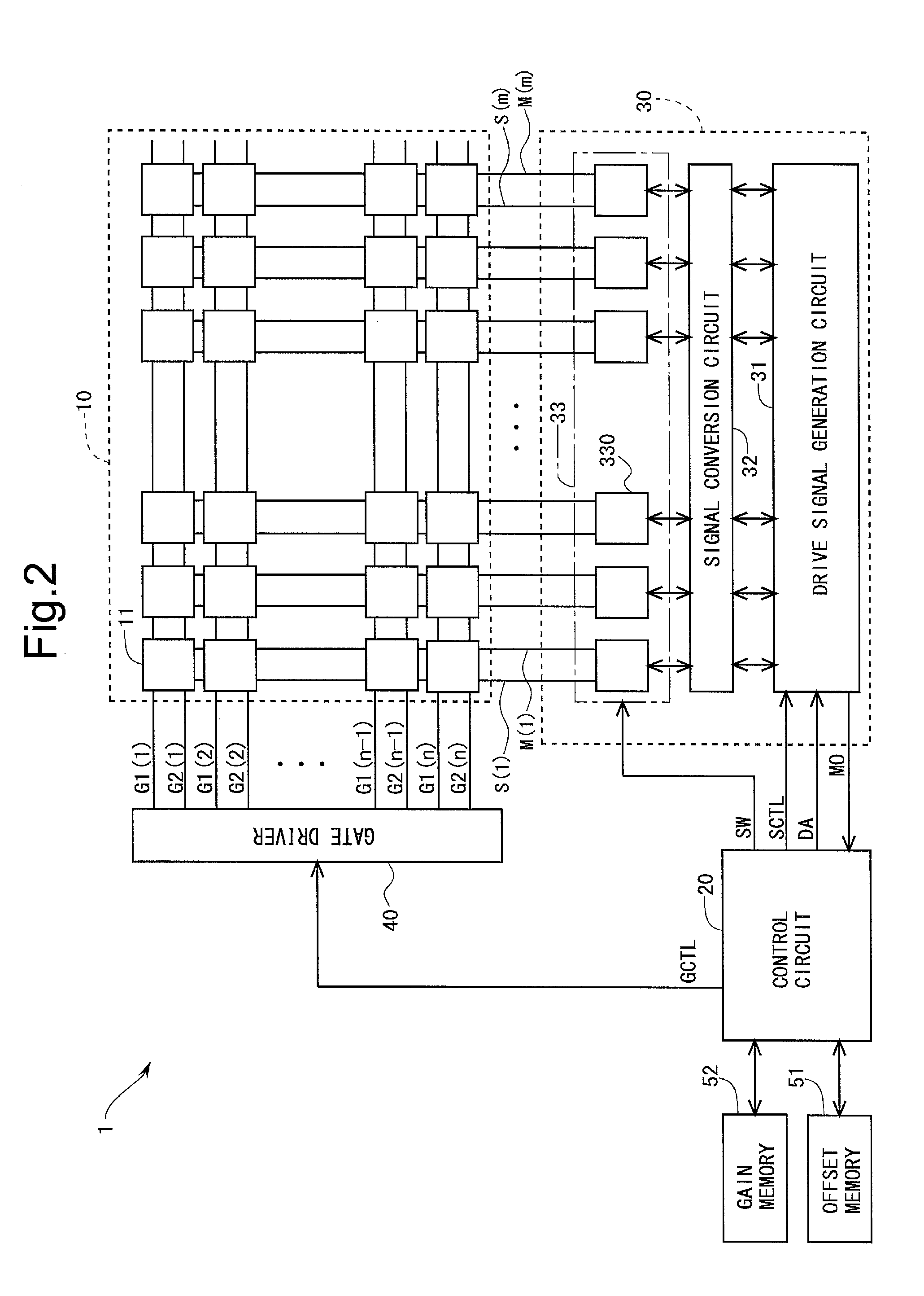
[0159]FIG. 2 is a block diagram showing an overall configuration of an active matrix-type organic EL display device 1 according to a first embodiment of the present invention. This organic EL display device 1 includes: a display unit (organic EL panel) 10; a control circuit 20; a source driver (data line drive circuit) 30; a gate driver (scanning line drive circuit) 40; an offset memory 51; and a gain memory 52. Note that a configuration in which either one or both of the source driver 30 and the gate driver 40 are formed integrally with the display unit 10 may be adopted. Moreover, the offset memory 51 and the gain memory 52 may be physically composed of one memory.

[0160]Note that, in this embodiment, a control unit is realized by the control circuit 20, a pixel circuit drive unit is realized by the source driver 30 and the gate driver 40, and a correction data storage unit is realized by the offset memory 51 and the gain memory 52.

[0161]...

modification examples

1.5 Modification Examples

[0236]A description is made below of modification examples of the above-described first embodiment. Note that, in the following, a description is made in detail only of different points from those of the first embodiment, and a description of similar points to those of the first embodiment is omitted.

first modification example

1.5.1 First Modification Example

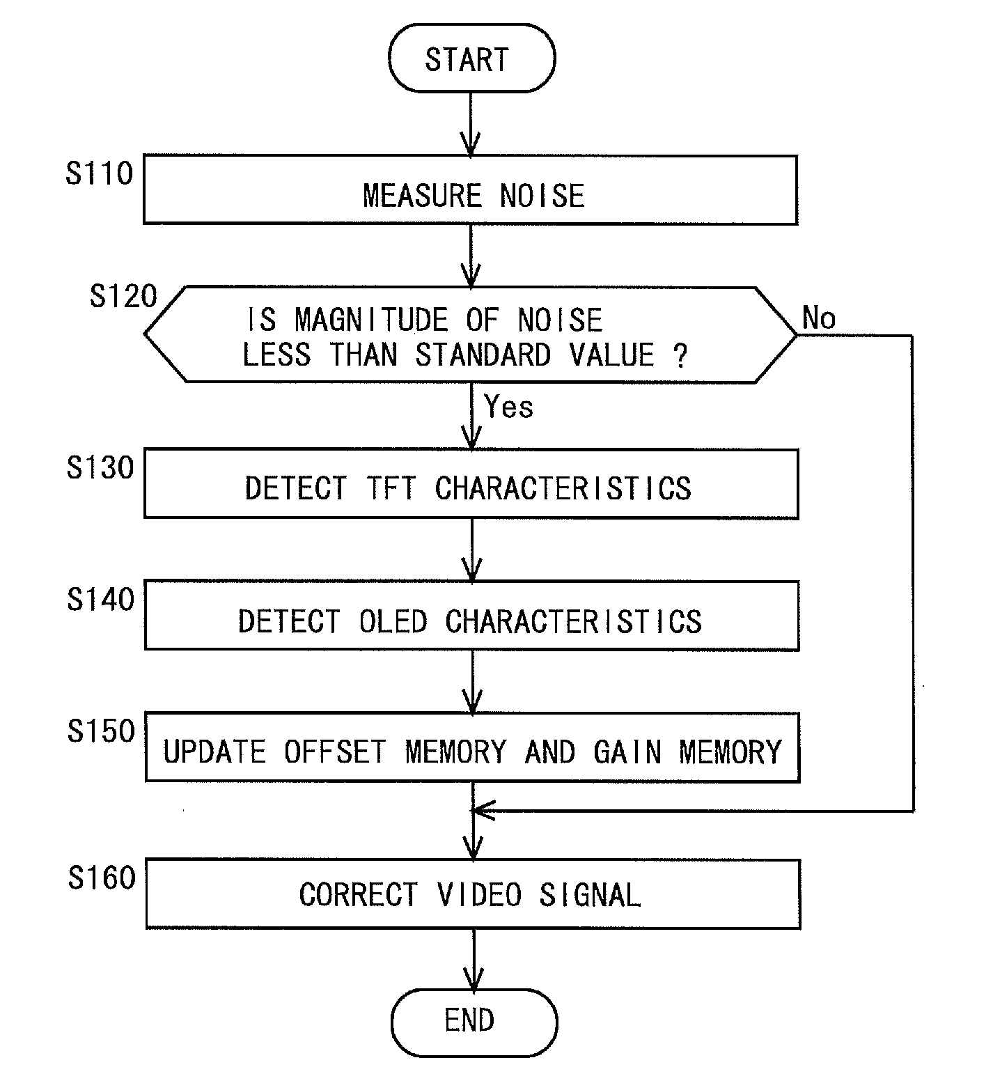
[0237]In the above-described first embodiment, with regard to the monitor column, in the case where the noise with the standard value or more is detected in the noise measurement period Tn, the TFT characteristics and the OLED characteristics are not detected. However, the present invention is not limited to this. The configuration may be such that the TFT characteristics and the OLED characteristics are detected irrespective of the magnitude of the noise detected in the noise measurement period Tn, and that the correction data is not updated in the case where the noise with the standard value or more is detected in the noise measurement period Tn (This is a configuration of this modification example).

[0238]FIG. 28 is a flowchart for explaining an outline of a drive method when focusing on the monitor column in the monitor rows in this modification example. At a beginning of the frame period, the noise generated in the monitor line M is measured (Step...


PUM


Abstract

In a display device having a pixel circuit including an electro-optical element in which brightness is controlled by a current, and including a drive transistor for controlling a current to be supplied to the electro-optical element, a drive method therefor includes: a noise measurement step of measuring noise; characteristic detection steps of detecting characteristics of the drive transistor and the electro-optical element; a correction data update step of updating correction data, which serves for correcting a video signal, based on detection results in the characteristic detection step; and a video signal correction step of correcting the video signal based on the correction data. When noise with a standard value or more is detected in the noise measurement step, processing of the correction data update step is not performed.

Description

TECHNICAL FIELD[0001]The present invention relates to a display device and a drive method for the same, and more specifically, relates to a display device including a pixel circuit having an electro-optical element such as an organic EL (Electro Luminescence) element, and to a drive method for the same.BACKGROUND ART[0002]Heretofore, as a display element which the display device includes, there are: an electro-optical element in which brightness is controlled by a voltage applied thereto; and an electro-optical element in which brightness is controlled by a current flowing therethrough. As a representative example of the electro-optical element in which the brightness is controlled by the voltage applied thereto, a liquid crystal display element is mentioned. Meanwhile, as a representative example of the electro-optical element in which the brightness is controlled by the current flowing therethrough, an organic EL element is mentioned. The organic EL element is also referred to as ...

Claims


Application Information

Patent Timeline
Patent Type & Authority Applications(United States)
IPC IPC(8): G09G3/32G09G3/00
CPCG09G3/3233G09G2300/0404G09G2310/08G09G3/006G09G2300/0842G09G2310/021G09G2310/0218G09G2320/0295G09G2320/043G09G2320/045
Inventor KISHI, NORITAKANOGUCHI, NOBORUYAMANAKA, SHIGETSUGUOHARA, MASANORI
Owner SHARP KK
Why Eureka
Try Eureka