Nitride Semiconductor Light Emitting Device and Fabrication Method Thereof

a light emitting device and nitride technology, applied in semiconductor/solid-state device manufacturing, semiconductor devices, electrical devices, etc., can solve the problems of poor reliability of the device, complex fabrication technique, drawbacks of growth techniques, etc., to improve the optical power and reliability of the light emitting device, reduce the crystallinity of the active layer, and improve the effect of the active layer crystallinity

Active Publication Date: 2008-06-19
SUZHOU LEKIN SEMICON CO LTD
View PDF5 Cites 76 Cited by
  • Summary
  • Abstract
  • Description
  • Claims
  • Application Information

AI Technical Summary

Benefits of technology

[0020]According to the present invention, the crystal defects of the nitride semiconductor light emitting device are decreased, the crystallinity of the active layer, and the optical power and reliability of the light emitting device can be enhanced.

Problems solved by technology

However, these growth techniques have a drawback such as the complexity in the fabrication technique.
The crystal defects are generated in various types propagated to a surface of the light emitting device, such as ‘threading dislocation’, ‘screw dislocation’, ‘line dislocation’, ‘point defect’, or ‘mixture’, which badly influences the device reliability.
For example, when a high voltage such as ESD or the like is instantly applied, the active layer is destroyed or the optical power is lowered.
The above problems provide fundamental reasons badly influencing the reliability.

Method used


Image

  • Nitride Semiconductor Light Emitting Device and Fabrication Method Thereof
  • Nitride Semiconductor Light Emitting Device and Fabrication Method Thereof
  • Nitride Semiconductor Light Emitting Device and Fabrication Method Thereof

Examples


Embodiment Construction

[0025]Hereinafter, embodiments of the present invention will be described in more detail with reference to the accompanying drawings.

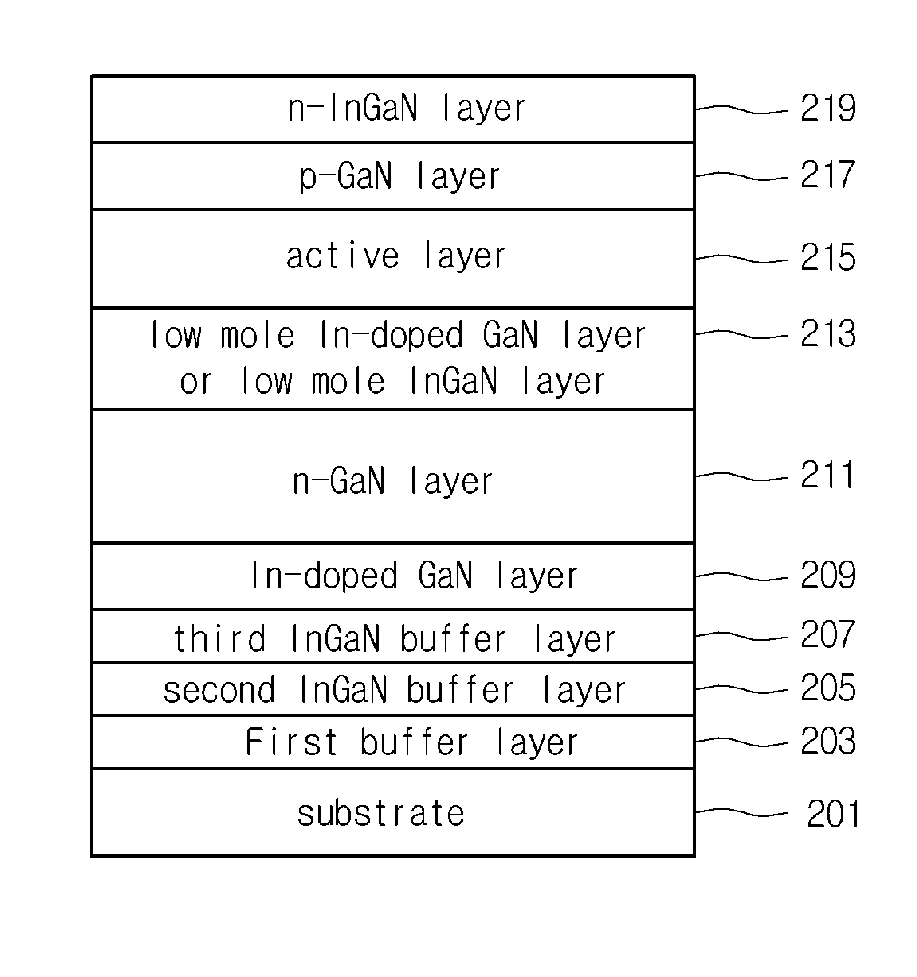
[0026]FIG. 2 is a sectional view of a nitride semiconductor light emitting device according to the present invention.

[0027]Referring to FIG. 2, the nitride semiconductor light emitting device of the present invention includes a substrate 201, a first buffer layer 203, a second InGaN buffer layer 205, a third InGaN buffer 207, an In-doped GaN layer 209, an n-GaN layer 211, a low-mole In-doped GaN layer or low-mole InGaN layer 213, an active layer 215, a p-GaN layer 217, and an n-InGaN layer 219.

[0028]The aforementioned layers will be described in more detail. First, the first buffer layer 203 is grown in a low temperature range of 500-600° C. on the substrate 201, for example, sapphire substrate. The first buffer layer 203 can be formed in one selected from the group consisting of a stack structure of AlInN / GaN, a super lattice structure of InGaN / GaN, a...


PUM


Abstract

Provided is a nitride semiconductor light emitting device including: a first nitride semiconductor layer; an active layer formed above the first nitride semiconductor layer; and a delta doped second nitride semiconductor layer formed above the active layer. According to the present invention, the optical power of the nitride semiconductor light emitting device is enhanced, optical power down phenomenon is improved and reliability against ESD (electro static discharge) is enhanced.

Description

TECHNICAL FIELD[0001]The present invention is relative to a nitride semiconductor light emitting device and fabrication method thereof, and to a nitride semiconductor light emitting device and fabrication method thereof in which optical power and reliability are enhanced.BACKGROUND ART[0002]A schematic stack structure of a general nitride semiconductor light emitting device and a fabrication method thereof will now be described.[0003]FIG. 1 is a sectional view of a general nitride semiconductor light emitting device.[0004]Referring to FIG. 1, a conventional nitride semiconductor light emitting device includes a substrate 101, a buffer layer 103, an n-GaN layer 105, an active layer 107 and a p-GaN layer 109.[0005]Herein, in order to minimize the occurrence of crystal defects due to differences in the lattice constants and the thermal expansion coefficients of the substrate 101, for example, sapphire substrate, and the n-GaN layer 105, a GaN-based nitride or an AlN-based nitride havin...

Claims


Application Information

Patent Timeline
Patent Type & Authority Applications(United States)
IPC IPC(8): H01L33/00H01L29/06H01L21/02H01L33/04H01L33/12H01L33/32H01L33/42
CPCH01L33/12H01L33/007
Inventor LEE, SUK HUN
Owner SUZHOU LEKIN SEMICON CO LTD
Why Eureka
Try Eureka