
Method for memory cell characterization using universal structure

a memory cell and universal structure technology, applied in the field of integrated circuits, can solve the problems of inability to obtain local mismatch information of the circuit elements of the memory cell, occupying a large fraction of the integrated circuit area, and a large amount of effort is usually spent to minimize the area of the memory cell

Active Publication Date: 2008-06-19
TEXAS INSTR INC
View PDF5 Cites 14 Cited by
  • Summary
  • Abstract
  • Description
  • Claims
  • Application Information

AI Technical Summary

Benefits of technology

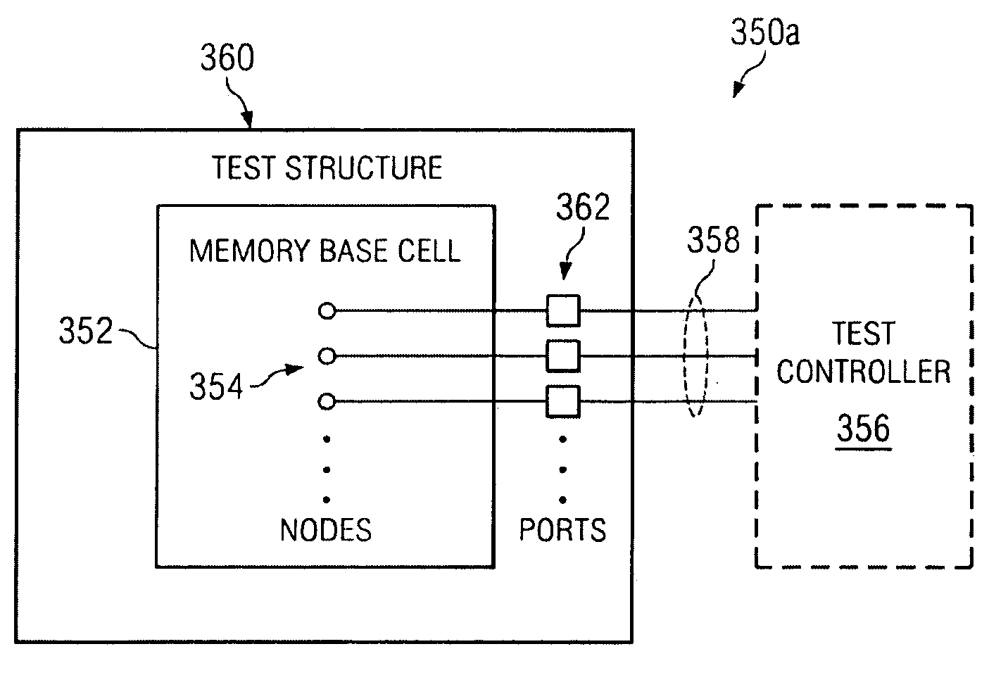
[0009]To address the above deficiencies in the art for memory cell characterization, it is an object of the present invention to provide a universal test structure (UTS) and an associated test method such that all characteristics required for a relatively complete characterization of a memory cell in an integrated circuit can be accurately measured from a same memory base cell. It is an advantage of the present invention to allow direct correlation among all the characteristics measured for a relatively complete characterization of memory cell. It is a further advantage of the present invention to allow collection of all the local mismatch data for a relatively complete characterization of a memory cell. It is a purpose of this invention to improve the usefulness of the measurements for memory cell development as well as for associated integrated circuit process and design development, monitoring, and control.
[0010]These and other objects, purposes, and advantages are provided in a test method comprising (a) providing an integrated circuit, wherein the integrated circuit comprises a memory base cell, wherein the memory base cell comprises a first storage node set, a second storage node set, a set of other nodes, and a set of circuit elements each having a plurality of terminals, wherein the set of other nodes comprises a first data node for accessing the first storage node set. The integrated circuit further comprises a first access control node for controlling the access of the first storage node set, a first supply node for supplying the first storage node set, and a second supply node for supplying the second storage node set, wherein the first and second supply nodes are of the same sinking or sourcing type. The method further comprises (b) conducting a circuit element test on a circuit element in the set of circuit elements, where in the circuit element test the first and second supply nodes are not connected together, each terminal of the circuit element is directly forced with an electrical quantity, and an electrical quantity is directly measured from a terminal of the circuit element, and (c) conducting at least one of a static noise margin test and a full cell test on the memory base cell.
[0011]In another aspect of the present invention, a test method is disclosed. The test method comprises (a) providing an integrated circuit, wherein the integrated circuit comprises a memory base cell, wherein the memory base cell comprises a first storage node set, a set of other nodes, and a plurality of circuit elements each having a plurality of terminals, wherein the first storage node set is the only storage node set in the memory base cell, wherein the set of other nodes comprises a first data node for accessing the first storage node set, a first access control node for controlling the access of the first storage node set, and a reference node for the first storage node set. The method further comprises (b) conducting a circuit element test on each circuit element in the set of circuit elements, each terminal of the each circuit element is directly forced with an electrical quantity, and an electrical quantity is directly measured from a terminal of the each circuit element.

Problems solved by technology

They often take a large fraction of integrated circuit area.
Consequently, significant amount of effort is usually spent to minimize the area of a memory cell while meeting the required performance and yield targets of the memory cell.
Also, the local mismatch information of the circuit elements of the memory cell cannot be obtained.
Therefore, the current approach to memory cell characterization limits the usefulness of the measurements for memory cell development and for integrated circuit process development and monitoring.

Method used


Image

  • Method for memory cell characterization using universal structure
  • Method for memory cell characterization using universal structure
  • Method for memory cell characterization using universal structure

Examples


Embodiment Construction

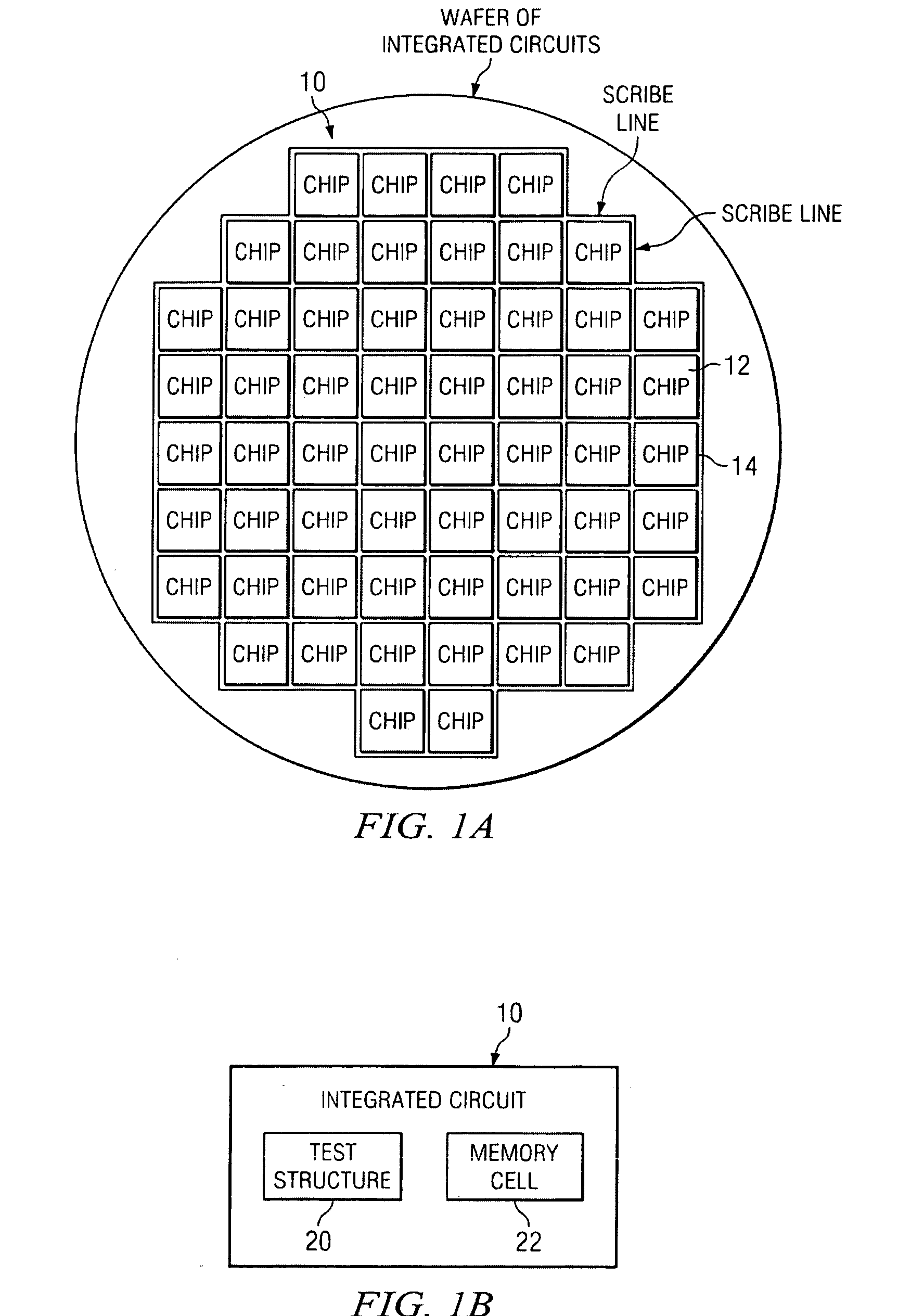
[0064]FIG. 1A is a diagram illustrating the relationship among an integrated circuit 10, a chip 12, and a scribe line 14.

[0065]The term “integrated circuit” used here includes both chip and scribe line regions. In particular, it includes test structures that are in a chip or in a scribe line.

[0066]The term “scribe line” refers to the region surrounding a chip and between chips where a saw can pass when sawing chips apart. Typically, some test structures are placed in a scribe line for characterizing circuits in a chip and for monitoring and control of the integrated circuit process.

[0067]FIG. 1B is a diagram illustrating the relationship among an integrated circuit 10, a test structure 20, and a memory cell 22 the test structure characterizes. In general, a test structure 20 and a circuit (such as the memory cell 22) the test structure characterizes can be independently placed in any regions of an integrated circuit 10.

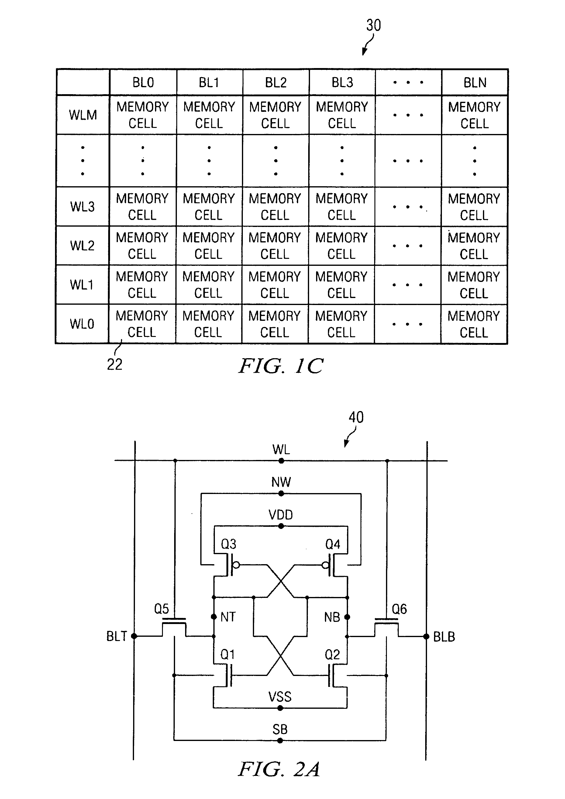
[0068]FIG. 1C is a diagram illustrating a plurality of memory ce...


PUM


Abstract

A test method includes providing an integrated circuit, where the integrated circuit includes a memory base cell, where the memory base cell includes a first storage node set, a second storage node set, a set of other nodes, and a set of circuit elements each having a plurality of terminals, where the set of other nodes includes a first data node for accessing the first storage node set, a first access control node for controlling the access of the first storage node set, a first supply node for supplying the first storage node set, and a second supply node for supplying the second storage node set, where the first and second supply nodes are of the same sinking or sourcing type. The method further includes conducting a circuit element test on a circuit element in the set of circuit elements, where in the circuit element test the first and second supply nodes are not connected together, each terminal of the circuit element is directly forced with an electrical quantity, and an electrical quantity is directly measured from a terminal of the circuit element. Further, the method includes conducting at least one of a static noise margin test or a full cell test on the memory base cell.

Description

REFERENCE TO RELATED APPLICATIONS[0001]This application claims priority to Ser. No. 60 / 874,768 filed Dec. 14, 2006, which is entitled “Universal Structure for Memory Cell Characterization.”FIELD OF INVENTION[0002]The present invention relates to integrated circuits and more particularly to structures and test methods for characterizing memory cells in integrated circuits.BACKGROUND OF THE INVENTION[0003]Memory cells are frequently used in integrated circuits. They often take a large fraction of integrated circuit area. Consequently, significant amount of effort is usually spent to minimize the area of a memory cell while meeting the required performance and yield targets of the memory cell. Typically, this involves not only the memory cell development but also the integrated circuit process development, since the area, performance, and yield of the memory cell strongly depend on the capability and variation of the integrated circuit process.[0004]Memory cell characterization provide...

Claims


Application Information

Patent Timeline
Patent Type & Authority Applications(United States)
IPC IPC(8): G11C29/08G06F11/26
CPCG11C11/413G11C29/006G11C2029/0403H01L27/11807H01L27/0207H01L27/11H01L27/1104H01L22/34H10B10/00H10B10/12
Inventor DENG, XIAOWEILOH, WAH KIT
Owner TEXAS INSTR INC
Learn More