

Substrate processing apparatus, focus ring heating method, and substrate processing method
- Summary
- Abstract
- Description
- Claims
- Application Information
AI Technical Summary
Benefits of technology
Problems solved by technology
Method used
Image

Examples
Embodiment Construction
[0053]The present invention will now be described with reference to the drawings showing a preferred embodiment thereof.
[0054]First, a description will be given of a substrate processing apparatus according to the embodiment.
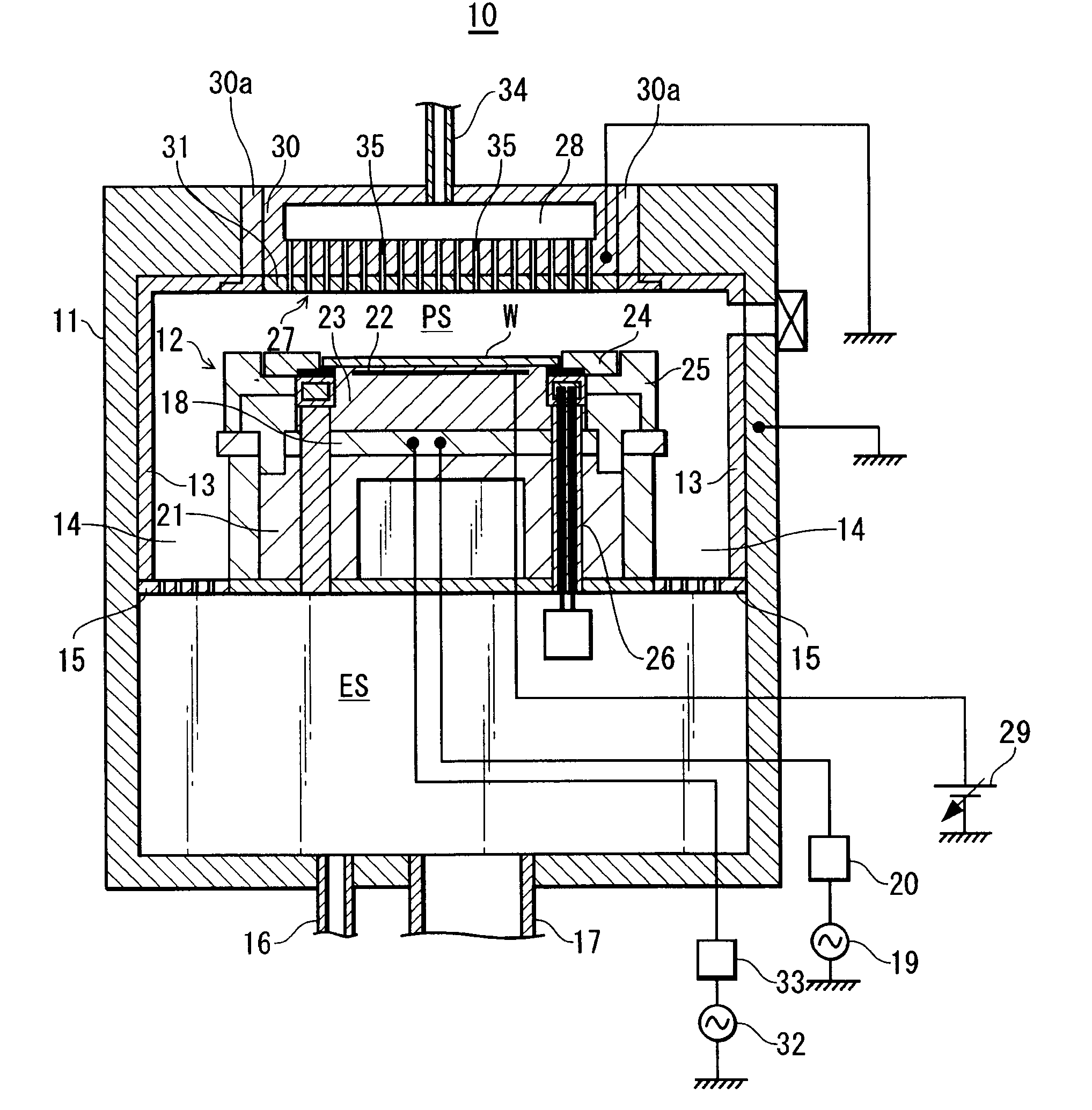
[0055]FIG. 1 is a sectional view schematically showing the construction of the substrate processing apparatus according to the present embodiment. The substrate processing apparatus according to the present embodiment is adapted to subject semiconductor wafers W as substrates to RIE (Reactive Ion Etching) processing.
[0056]As shown in FIG. 1, the substrate processing apparatus 10 is comprised of a cylindrical housing chamber 11 that has a processing space PS in an upper part thereof. In the processing space PS, plasma is produced as will be described later. Moreover, the substrate processing housing chamber 11 has disposed therein a cylindrical susceptor 12 as a stage on which is mounted a semiconductor wafer W (hereinafter referred to merely as a “wafer W”) havi...
PUM
| Property | Measurement | Unit |
|---|---|---|
| Temperature | aaaaa | aaaaa |
| Pressure | aaaaa | aaaaa |
| Magnetic field | aaaaa | aaaaa |
Abstract
Description
Claims
Application Information