Semiconductor Device and Driving Method Thereof

a technology of mikro-onductors and driving methods, which is applied in the field of mikro-onductors, can solve the problems of unstable supply of electric power to the wireless tag, unstable voltage vddb>1/b> generated in the power supply generation portion and the vddb>2/b> obtained by boosting up the voltage vddb>1/b>, and achieve stable voltage and control of voltage variation. , the effect o

Inactive Publication Date: 2008-06-26
SEMICON ENERGY LAB CO LTD
View PDF20 Cites 20 Cited by
  • Summary
  • Abstract
  • Description
  • Claims
  • Application Information

AI Technical Summary

Benefits of technology

[0019]The present invention makes it possible to control variation in a voltage after being boosted up due to a modulation of radio wave and to supply a stable voltage to a memory by operating a semiconductor device with dividing periods into a period of a signal transmission from a reader / writer and a period of boosting up a voltage. As a result, writing data into the memory can be stably conducted, whereby malfunction of the memory can be prevented.
[0020]Further, in the present invention, since a variation in voltage after being boosted up due to a modulation of a radio wave can be controlled, it is not required to adapt a boosting capability of a boosting circuit to minimum in the expectation of variation in a voltage. Thus, power consumption of the semiconductor device can be reduced.

Problems solved by technology

However, there has been a problem in that supply of electric power to the wireless tag tends to be unstable when a radio wave generated from the reader writer is modulated in order to perform communication from the reader / writer to the wireless tag. FIG. 17 shows a timing chart for boosting up a voltage supplied to the memory in parallel with performing communication from the reader / writer to the wireless tag. FIG. 17 shows, from the top, a change versus time in an alternating voltage generated by the antenna, a change versus time in a voltage before being boosted up VDD1 obtained by rectification of the alternating voltage, and a change versus time in a voltage VDD2, which is a voltage after being boosted up and supplied to the memory.
As can be seen in FIG. 17, when communication from the reader / writer to the wireless tag is performed, the voltage VDD1 generated in a power supply generation portion and the VDD 2 obtained by boosting up the voltage VDD1 tend to be unstable.
Even if decrease in supply capability of a voltage in the power supply generation portion in the wireless tag is compensated by a storage capacitor, completely stable supply of a voltage has been impossible.
Consequently, in the case of writing data into the memory in parallel with communication from the reader / writer to the wireless tag, it is difficult to secure a stable voltage for writing even if a boosting circuit is employed for boosting up a voltage.

Method used


Image

  • Semiconductor Device and Driving Method Thereof
  • Semiconductor Device and Driving Method Thereof
  • Semiconductor Device and Driving Method Thereof

Examples


embodiment mode 1

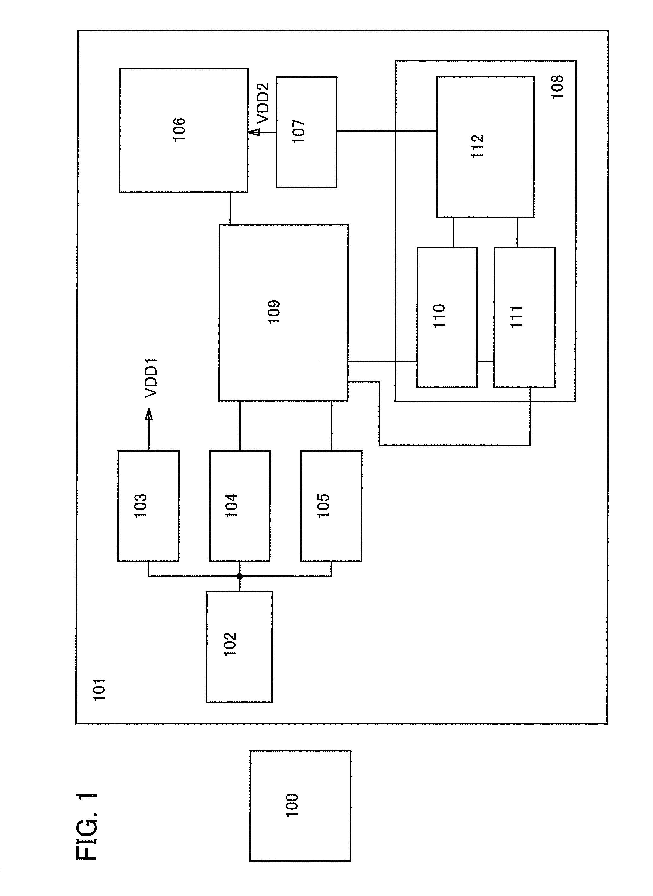
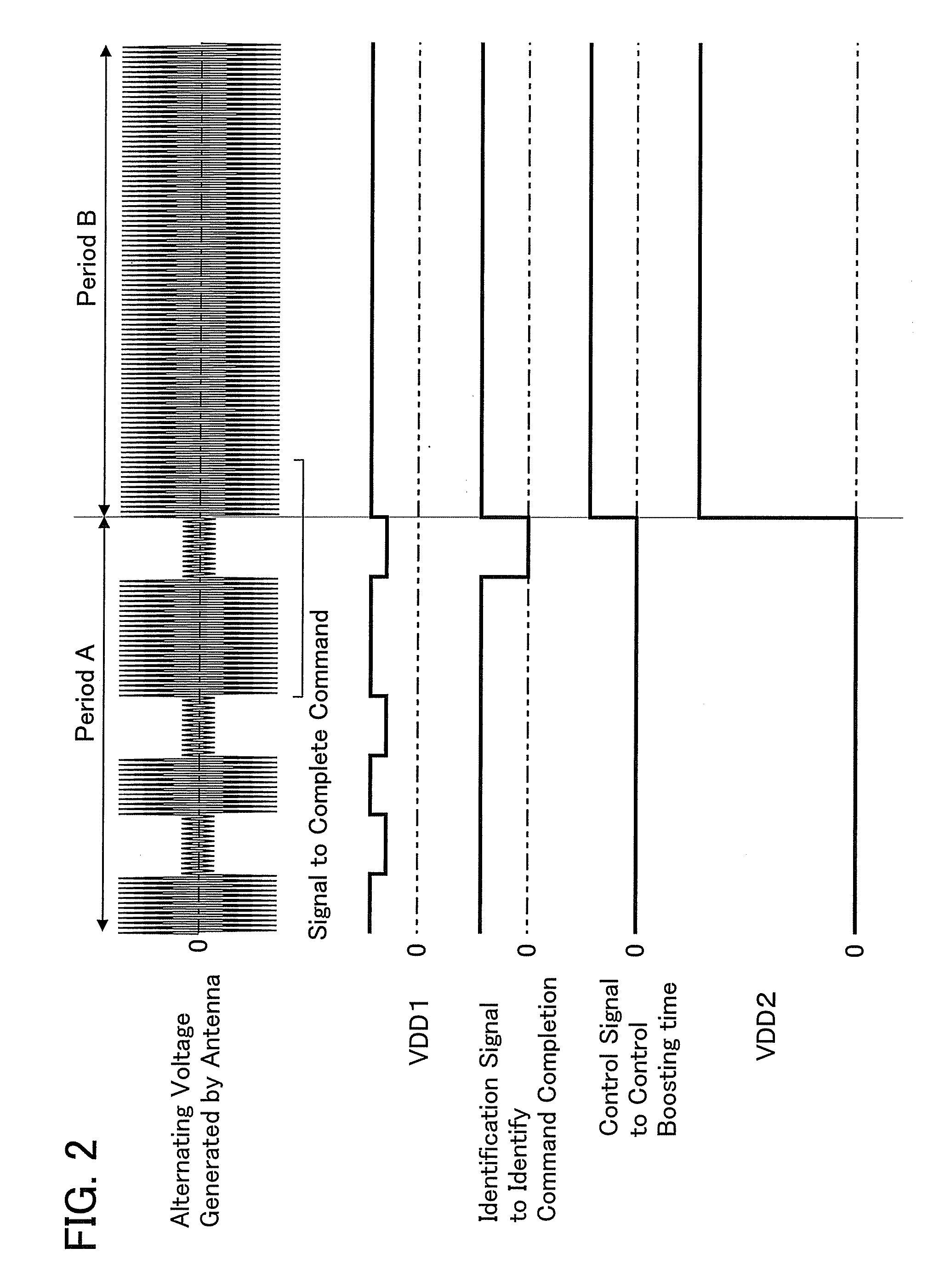
[0042]FIG. 1 shows a block diagram of a reader / writer 100 and a semiconductor device 101 of the present invention conducting wireless communication with the reader / writer 100.

[0043]The semiconductor device 101 includes the following: an antenna circuit 102 to receive a radio wave from the reader / writer 100 exchanging information with the semiconductor device 101; a power supply generation circuit 103 in which an alternating voltage generated by receiving a radio wave in the antenna circuit 102 is rectified into a direct voltage so that the direct voltage is supplied to various circuits in the semiconductor device 101; a demodulation circuit 104 to extract information which is included in the radio wave received in the antenna circuit 102; a modulation circuit 105 to modulate a radio wave for transmitting information from the semiconductor device 101 to the reader / writer 100; a memory 106 capable of storing data; a boosting circuit 107 for boosting a voltage supplied to the memory 10...

embodiment mode 2

[0066]In this embodiment mode, an example of a concrete circuit structure of boosting possibility a circuit for identification of boosting possibility will be described.

[0067]FIG. 11 shows a circuit diagram of boosting possibility a circuit for identification of boosting possibility. In this embodiment mode, the identification circuit to identify boosting possibility includes an AND circuit. Into each of the two input portions of the AND circuit, a control signal to control boosting time transmitted from a control circuit to control boosting time, and an identification signal to identify command completion transmitted from a identification circuit to identify command completion are inputted. Then, an identification signal to identify boosting possibility is outputted from the control circuit to control boosting time. Only when both the control signal to control boosting time and the identification signal to identify command completion which are inputted into the identification circu...

embodiment mode 3

[0068]In this embodiment mode, a structure of a semiconductor device of the present invention having a power storage means will be described.

[0069]FIG. 12 shows a block diagram of a semiconductor device 301 in this embodiment mode. The semiconductor device 301 includes the following: an antenna circuit 302; a power supply generation circuit 303; a demodulation circuit 304; a modulation circuit 305; a memory 306; a boosting circuit 307; a logic circuit 309; a boosting control portion 308; a charging / discharging control circuit 313; and a power storage means 314. The boosting control portion 308 includes a control circuit 310 for boosting time, an identification circuit 311 for command completion, and an identification circuit 312 for boosting possibility.

[0070]The antenna circuit 302 has an antenna and a resonant capacitor connected to the antenna in parallel. The antenna circuit 302 is capable of receiving a radio wave from a reader / writer 300 first, transmitting the received signal...


PUM


Abstract

To provide a semiconductor device, which is capable of supplying a stable voltage to a memory and communicating wirelessly in writing data into a memory, and a driving method thereof. The semiconductor device is operated with periods which are divided into a period for receiving a signal wirelessly from a reader/writer, and a period for boosting up electric power received wirelessly from the reader/writer before being supplied to the memory. The signals transmitted from the reader/writer include timing for completion of signal transmission as information. The timing for completion of signal transmission is known by receiving the signals. After completion of signal transmission from the reader/writer, electric power received from the reader/writer starts to be boosted up, and then it is supplied to the memory in the semiconductor device.

Description

BACKGROUND OF THE INVENTION[0001]1. Field of the Invention[0002]The present invention relates to a semiconductor device including a memory and having capability of performing wireless communication. In addition, the present invention relates to a driving method of the semiconductor device to determine timing of writing data into the memory.[0003]2. Description of the Related Art[0004]With development in computer technology, technology for information identification without contact has been a practical use and a memory performing a stable operation without contact has been needed. In response to such a demand, a wireless tag capable of communication without contact has been developed recently.[0005]Some wireless tags include a function of memories. The memories, for example, can store data specific to the wireless tags, and data of programs for operating integrated circuits inside the wireless tags.[0006]The wavelength of a radio wave transmitted and received between wireless tags an...

Claims


Application Information

Patent Timeline
Patent Type & Authority Applications(United States)
IPC IPC(8): G06K19/06G06K19/07
CPCG11C7/24G11C5/142G11C7/00
Inventor OHSHIMA, KAZUAKI
Owner SEMICON ENERGY LAB CO LTD
Why Eureka
Try Eureka