Light-emitting diode structure and method for manufacturing the same

Inactive Publication Date: 2008-07-03
EPISTAR CORP
View PDF6 Cites 13 Cited by
  • Summary
  • Abstract
  • Description
  • Claims
  • Application Information

AI Technical Summary

Benefits of technology

[0006]An aspect of the present invention is to provide a LED structure and a method for manufacturing the same, thereby making the epitaxial layers under two electrode pads have similar surface roughnesses for forming two electrode pads of similar lu

Problems solved by technology

However, the respective conditions are different for each product lot, so that the conventional method of adjusting the etch parameters is significantly limited and it is difficult to make the surface roughnesses of the epitaxial layers under these two electrode

Method used


Image

  • Light-emitting diode structure and method for manufacturing the same
  • Light-emitting diode structure and method for manufacturing the same
  • Light-emitting diode structure and method for manufacturing the same

Examples


Embodiment Construction

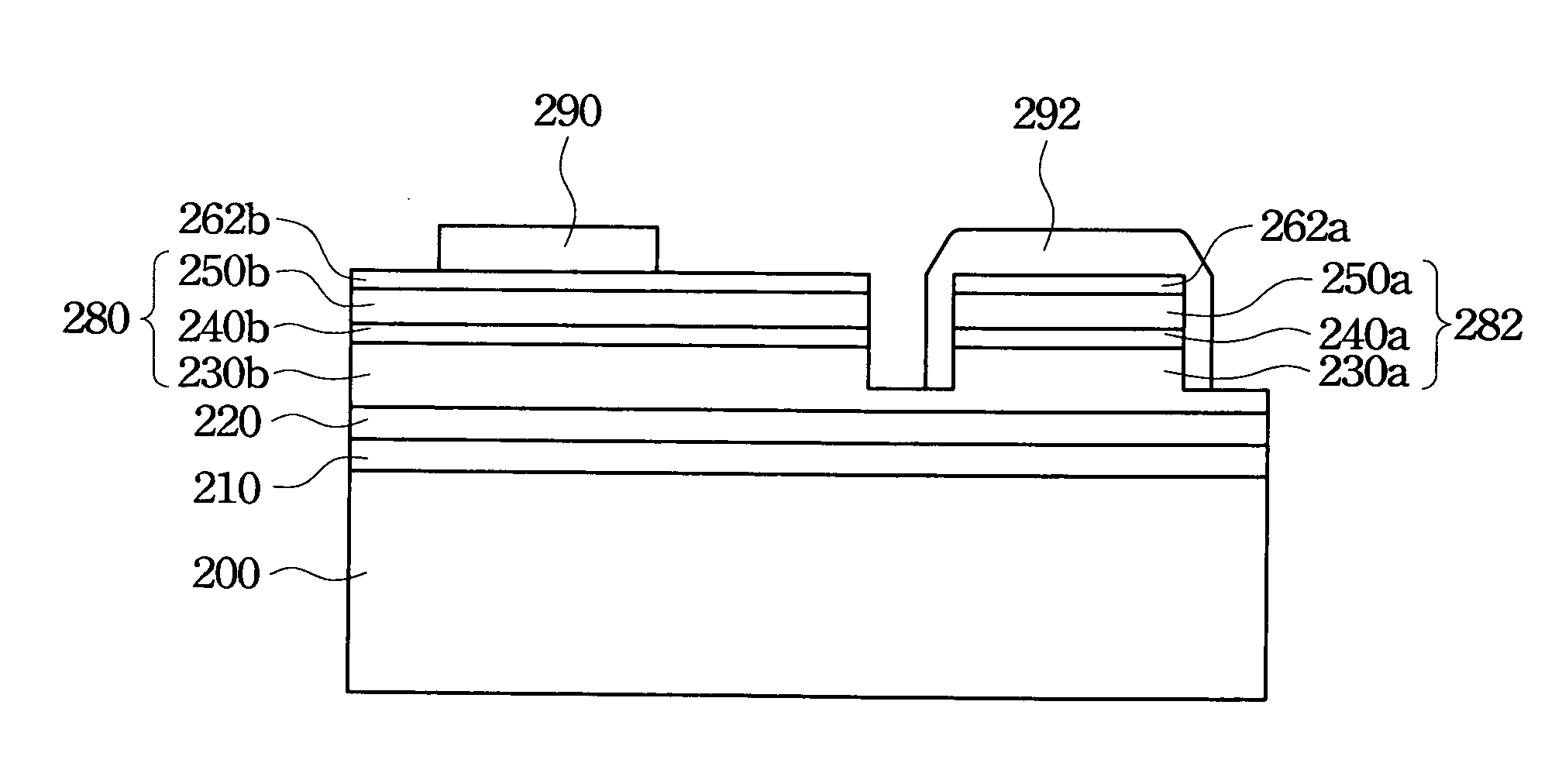
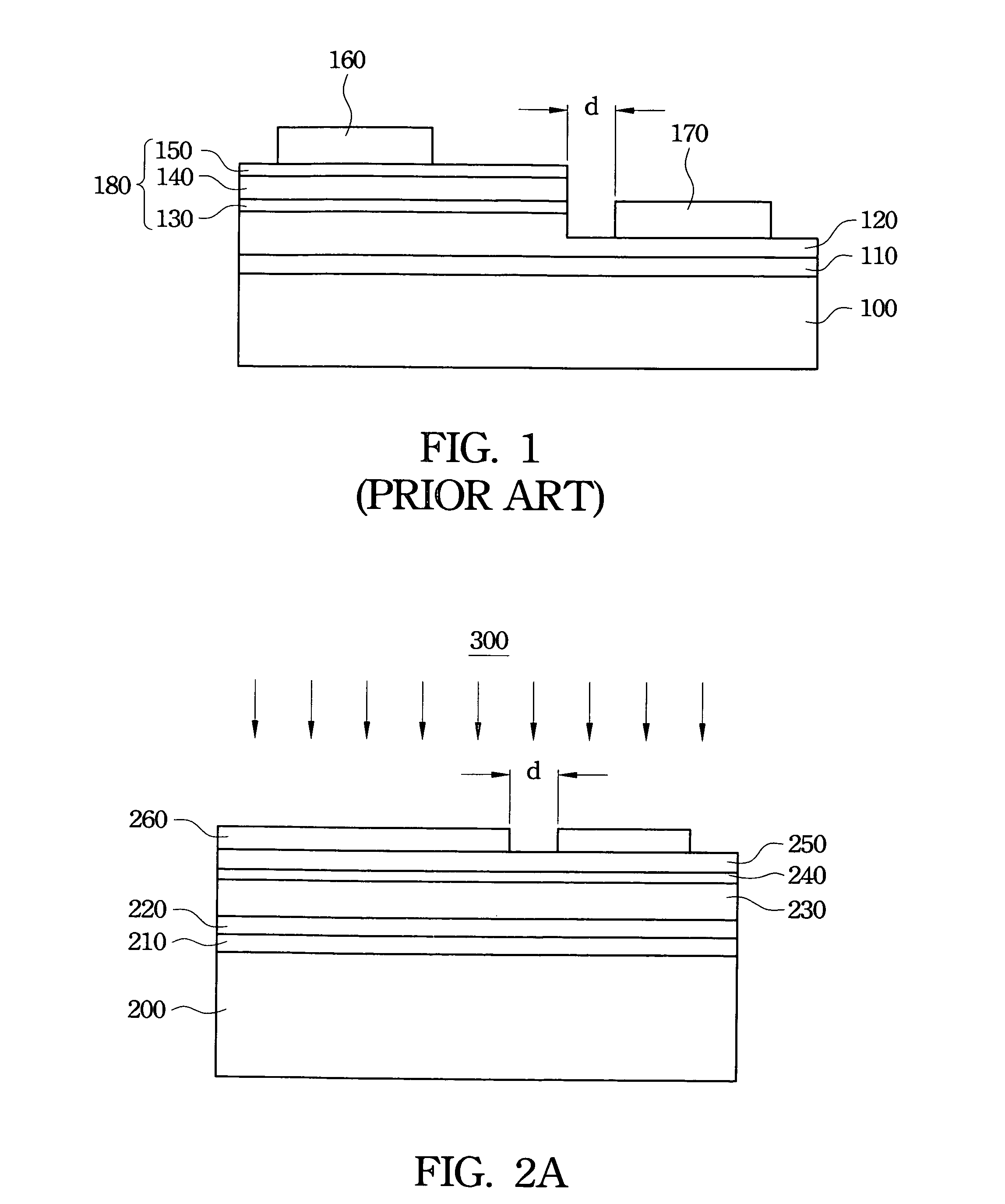
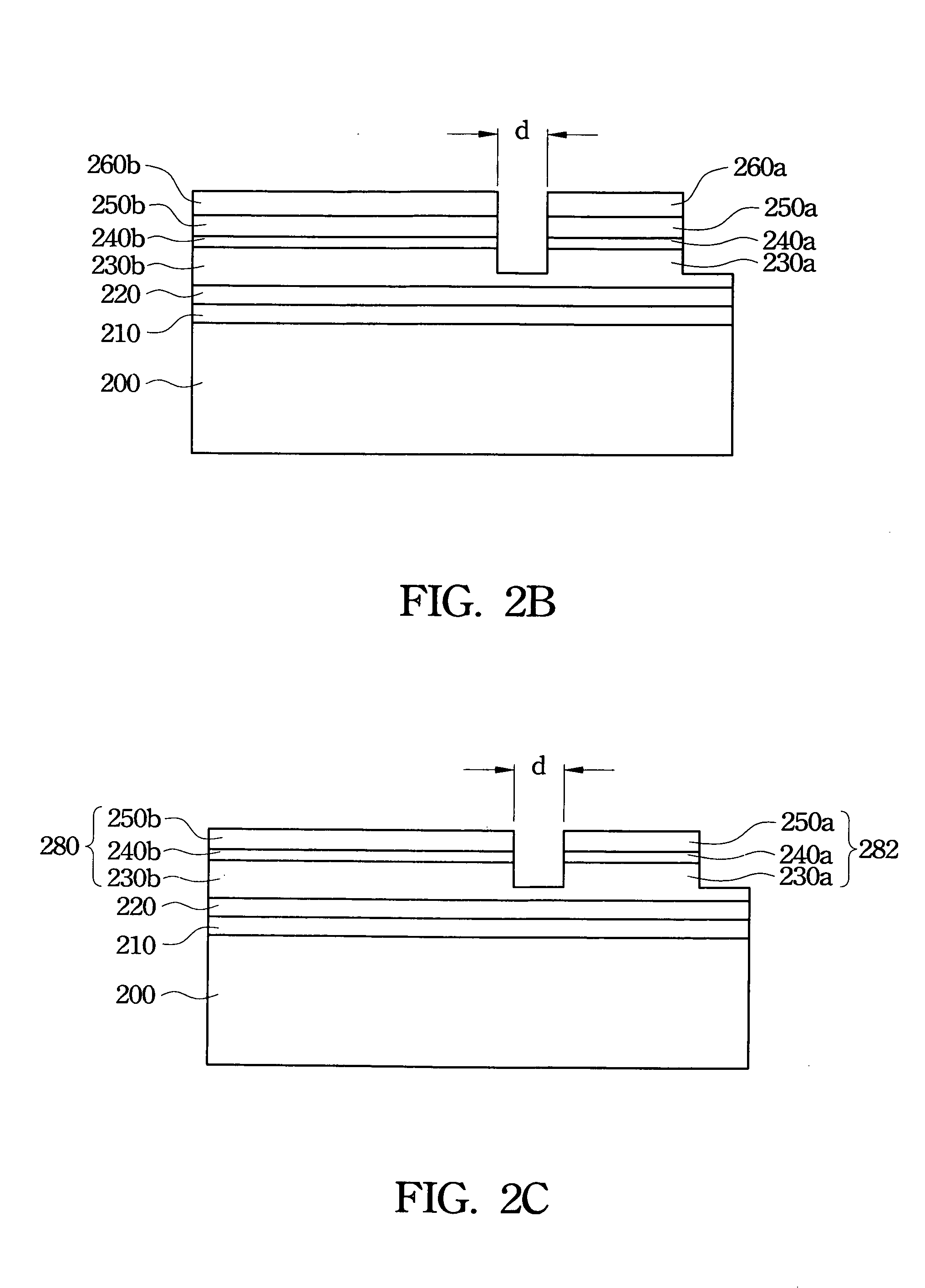
[0016]An embodiment of the present invention shown hereinafter is used to resolve the problem of poor image recognition and rough surface textures caused by different levels of surface roughness of the epitaxial layers under two respective electrode pads. The embodiment of the present invention reserves a complete epitaxial structure (protrusive structure) in the area under a n-type electrode pad, and the protrusive structure is substantially equivalent to a light-emitting epitaxial structure under a p-type electrode pad, wherein the thickness of the material layers forming the protrusive structure is smaller than or equal to the thickness of the material layers forming the light-emitting epitaxial structure, thereby making the surface roughnesses of the epitaxial layers under these two electrode pads as similar as possible, thus resolving the problem of rough surface textures. Moreover, a portion of the n-type electrode pad directly contacts a n-type epitaxial layer so as to assure...


PUM


Abstract

A light-emitting diode (LED) structure and a method for manufacturing the LED structure are disclosed for promoting the recognition rate of LED chips, wherein a roughness degree of the surface under a first electrode pad of a first conductivity type is made similar to that of the surface under a second electrode pad of a second conductivity type, so that the luster shown from the first electrode pad can be similar to that from the second electrode pad, thus resolving the poor recognition problem of wire-bonding machines caused by different lusters from the first and second electrode pads.

Description

RELATED APPLICATIONS[0001]The present application is based on, and claims priority from, Taiwan Application Serial Number 95150037, filed Dec. 29, 2006, the disclosure of which is hereby incorporated by reference herein in its entirety.FIELD OF THE INVENTION[0002]The present invention relates to a light-emitting diode (LED) structure and a method for manufacturing the same, and more particularly, to a LED structure and its manufacturing method for promoting the LED chip recognition rate.BACKGROUND OF THE INVENTION[0003]Referring to FIG. 1, FIG. 1 is a schematic cross-sectional view showing a conventional LED structure, wherein on a substrate 100, a buffer layer 110 and a n-type confining layer 120 are formed in sequence. An active layer 130, a p-type confining layer 140, a transparent electrode layer 150 and a p-type electrode pad 160 are formed on one portion of the n-type confining layer 120, and a n-type electrode pad 170 is formed on the other portion of the n-type confining lay...

Claims


Application Information

Patent Timeline
IPC IPC(8): H01L33/00H01L21/00H01L33/20H01L33/38
CPCH01L33/20H01L2933/0016H01L33/382H01L33/38
Inventor KUO, CHENG-TAYU, KUO-HUICHEN, CHAO-HSINGKO, TSUN-KAIHUANG, CHI-MINGYEH, SHIH-WEICHUNG, CHIEN-KAI
Owner EPISTAR CORP
Why Eureka
Try Eureka