Method of manufacturing circuit board embedding thin film capacitor

a thin film capacitor and manufacturing method technology, applied in the direction of fixed capacitors, dielectric characteristics, fixed capacitor details, etc., can solve the problems of board deformation, easy oxidation of copper foil, etc., and achieve the effect of minimizing damage to the dielectric layer

Inactive Publication Date: 2008-07-03
SAMSUNG ELECTRO MECHANICS CO LTD
View PDF6 Cites 25 Cited by
  • Summary
  • Abstract
  • Description
  • Claims
  • Application Information

AI Technical Summary

Benefits of technology

[0012]An aspect of the present invention provides a multilayer circuit board embedding a thin film capacitor in which a tran

Problems solved by technology

However, in the conventional capacitor embedded in the PCB, the insulating layer is formed of polymer and thus not capable of undergoing high temperature heat treatme

Method used


Image

  • Method of manufacturing circuit board embedding thin film capacitor
  • Method of manufacturing circuit board embedding thin film capacitor
  • Method of manufacturing circuit board embedding thin film capacitor

Examples


Embodiment Construction

[0030]Exemplary embodiments of the present invention will now be described in detail with reference to the accompanying drawings.

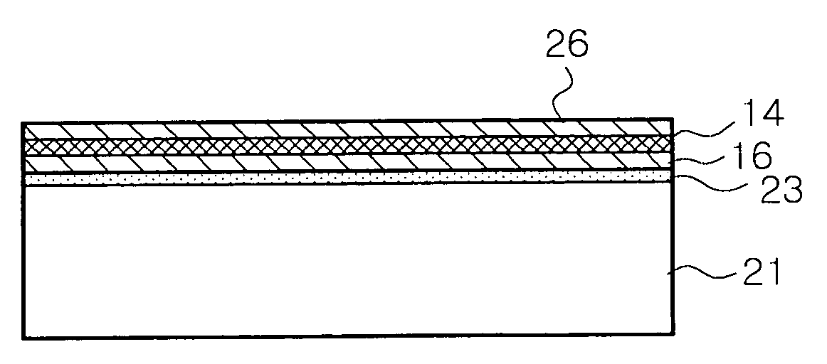
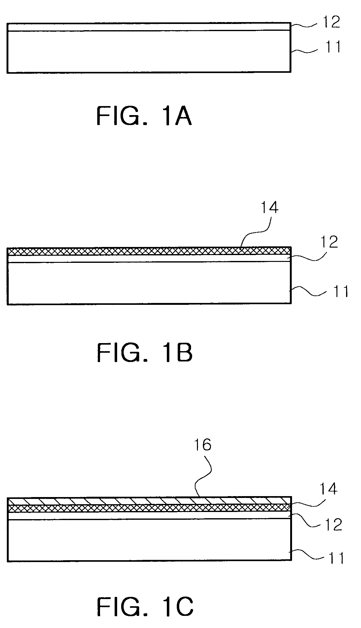
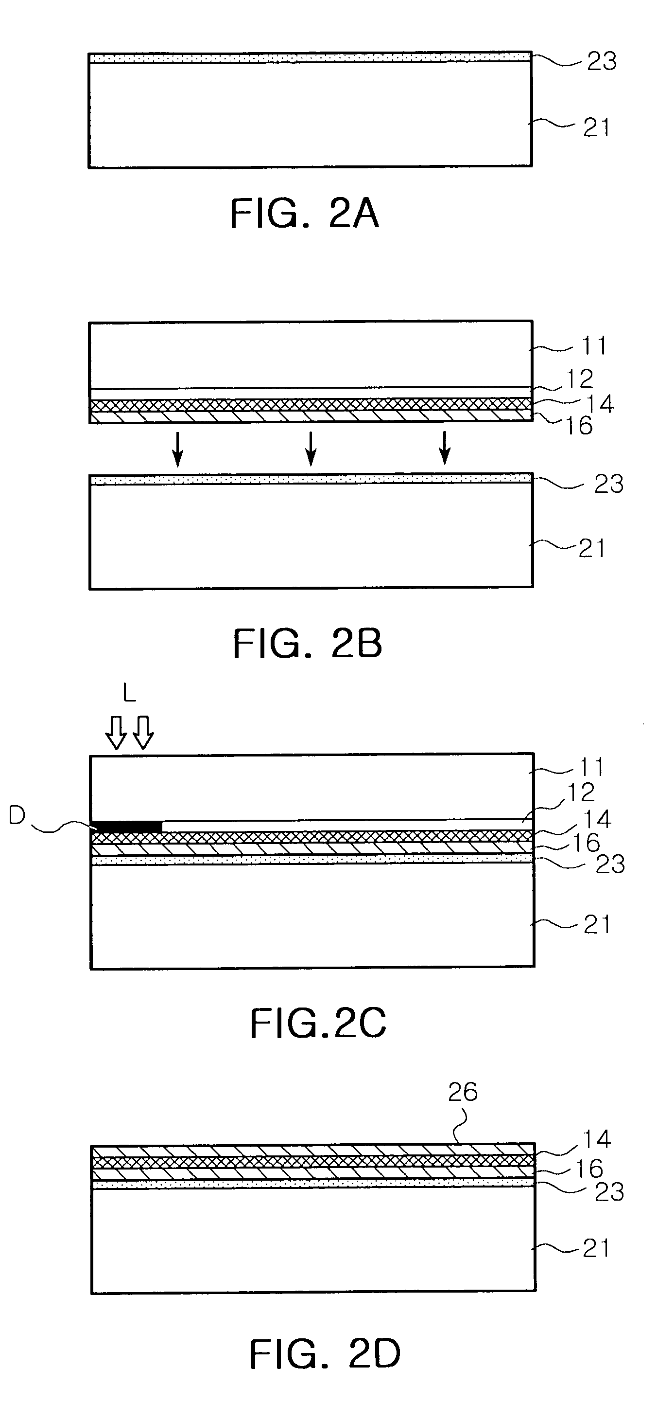
[0031]FIGS. 1A to 1C are procedural views for explaining a process for forming a transfer structure for a thin film capacitor employed in a method of manufacturing a circuit board embedding a thin film capacitor according to an exemplary embodiment of the invention.

[0032]As shown in FIG. 1A, the method of the present invention starts with forming a sacrificial layer 12 on a first substrate 11.

[0033]The “sacrificial layer 12” is a layer formed of a material decomposable by energy of a laser beam used. In a later process, the laser beam will penetrate the first substrate 11 to decompose the sacrificial layer.

[0034]To selectively remove the sacrificial layer 12, the laser beam may have a focal point thereof adjusted in such a way that energy of the laser beam is focused on the sacrificial layer 12. Particularly, materials for the first substrate 11 and the sa...


PUM

PropertyMeasurementUnit
Dielectric polarization enthalpyaaaaaaaaaa
Band gapaaaaaaaaaa
Electrical conductoraaaaaaaaaa

Abstract

A method of manufacturing a circuit board embedding a thin film capacitor, the method including: forming a sacrificial layer on a first substrate; forming a dielectric layer on the sacrificial layer; forming a first electrode layer on the dielectric layer; disposing the first substrate on the second substrate in such a way that the first electrode layer is bonded to a top of a second substrate; decomposing the sacrificial layer by irradiating a laser beam onto the sacrificial layer through the first substrate; separating the first substrate from the second substrate; and forming a second electrode layer on the dielectric layer.

Description

CROSS-REFERENCE TO RELATED APPLICATIONS[0001]This application claims the priority of Korean Patent Application No. 2006-137585 filed on Dec. 29, 2006, in the Korean Intellectual Property Office, the disclosure of which is incorporated herein by reference.BACKGROUND OF THE INVENTION[0002]1. Field of the Invention[0003]The present invention relates to a method of manufacturing a circuit board such as a printed circuit board, and more particularly, to a circuit board embedding a thin film capacitor in which the thin film capacitor is fabricated using a laser lift-off process.[0004]2. Description of the Related Art[0005]With a trend of smaller size, lighter weight, higher speed and higher frequency in electronic devices, the electronic devices are increasingly required to be highly integrated. To this end, vigorous studies have been conducted on technologies for integrating passive and active devices into a board to enhance efficiency.[0006]In related efforts to achieve smaller electron...

Claims


Application Information

Patent Timeline
IPC IPC(8): H01G4/00H05K3/30
CPCH01G4/005H01G4/33H05K1/162H05K3/046H05K2201/0108H05K2201/0175Y10T29/49155H05K2203/0528H05K2203/0537H05K2203/107Y10T29/49128Y10T29/49126Y10T29/4913H05K2203/016H01L21/3205H01L27/105
Inventor LEE, IN HYUNGCHUNG, YUL KYOKIM, BAE KYUNLEE, SEUNG EUNLEE, JUNG WON
Owner SAMSUNG ELECTRO MECHANICS CO LTD
Why Eureka
Try Eureka