Method, system, and computer program product for predicting thin film integrity, manufacturability, reliability, and performance in electronic designs

a technology of electronic design and manufacturability, applied in the direction of semiconductor/solid-state device testing/measurement, testing circuits, instruments, etc., can solve the problems of patchy solutions provided by conventional methods and systems without addressing the root causes of problems

Active Publication Date: 2008-07-03
CADENCE DESIGN SYST INC
View PDF33 Cites 43 Cited by
  • Summary
  • Abstract
  • Description
  • Claims
  • Application Information

AI Technical Summary

Problems solved by technology

As noted above, conventional methods and systems provide patchy solutions without addressing the root causes of the problem.

Method used


Image

  • Method, system, and computer program product for predicting thin film integrity, manufacturability, reliability, and performance in electronic designs
  • Method, system, and computer program product for predicting thin film integrity, manufacturability, reliability, and performance in electronic designs
  • Method, system, and computer program product for predicting thin film integrity, manufacturability, reliability, and performance in electronic designs

Examples


Embodiment Construction

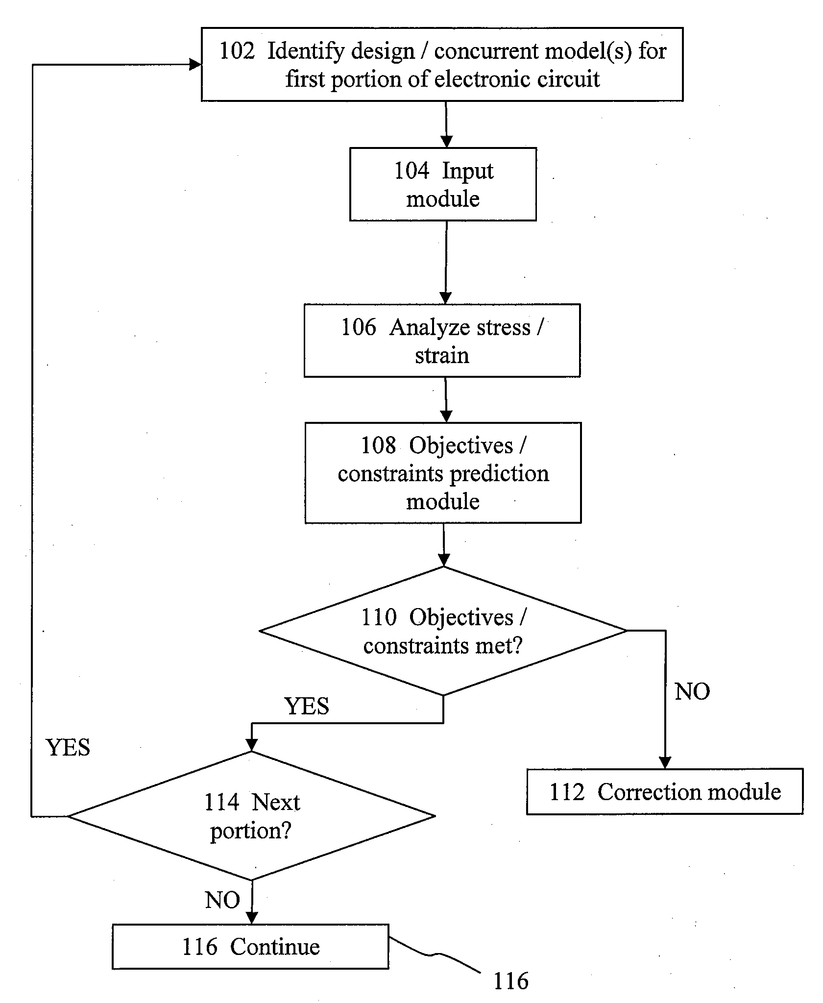
[0021]The present invention is directed to an improved method, system, and computer program product for evaluating the stresses or strains within various layers or parts of an integrated circuit or an electronic circuit with the aid of the one or more concurrent models for the manufacturing of the electronic circuit or the design layout to predict whether the electronic designs meet certain design criteria. Some embodiments utilize the above method, system, and / or computer program to evaluating stresses within various layers of an integrated circuit with the aid of the design layout and the one or more concurrent models for the manufacturing processes or techniques to compute the non-planarity of the films. As noted above, conventional methods and systems provide patchy solutions without addressing the root causes of the problem.

[0022]Referring to FIG. 1, the method or the system of several embodiments of the invention first identifies a first portion of the integrated circuit (IC) ...


PUM


Abstract

Disclosed is an improved method, system, and computer program product for predicting and improving the integrity, manufacturability, reliability, and performance of an electronic circuit feature based on the stresses or strains of design features of electronic designs. Some embodiments identify the design, the concurrent model(s), design feature physical or electrical parameters or attributes, analyzes the stresses or strains to predict the integrity of the design and determines whether the design meets the design objectives or constraints. Some other embodiments make corrections to the designs or the processes based upon the determination of whether the design meets the design objectives or constraints. Some other embodiments compute the variations of the design features as a result of the stresses or strains and determine their impact on the subsequent processes.

Description

CROSS-REFERENCE TO RELATED APPLICATION(S)[0001]This application claims the benefit of U.S. Provisional Application No. 60 / 878,005, filed on Dec. 29, 2006, which is hereby incorporated by reference in its entirety.BACKGROUND OF THE INVENTION[0002]Stresses and strains within a feature of an integrated circuit (IC) or an electronic circuit design may cause many undesired adverse effects or even cause the design to fail. Among the many adverse effects, manufacturability, reliability, and performance are of primary concern. For example, the electric stress in the gate oxide caused by the electric field across the oxide has been shown to increase as the voltage drop across the oxide increases; the stress also increases as the temperature rises due to Joule heating which may be further exacerbated due to the introduction of low-k dielectrics because of its higher porosity. The voltage overshoot during device switching further worsens the problem and increases the likelihood of gate oxide p...

Claims


Application Information

Patent Timeline
Patent Type & Authority Applications(United States)
IPC IPC(8): G01R31/26G01R27/28
CPCG06F17/5009G06F2217/80G06F2217/06G06F30/20G06F2111/04G06F2119/08
Inventor WHITE, DAVIDSCHEFFER, LOUIS K.
Owner CADENCE DESIGN SYST INC
Why Eureka
Try Eureka