Printed Wiring Board And Method Of Manufacturing Same

a technology of printed wiring board and manufacturing method, which is applied in the direction of printed circuit aspects, conductive pattern formation, electric connection formation of printed elements, etc., can solve the problems of shortening of vias, shortening of vias, and inability to narrow vias

Inactive Publication Date: 2008-07-10
IBM CORP
View PDF3 Cites 29 Cited by
  • Summary
  • Abstract
  • Description
  • Claims
  • Application Information

AI Technical Summary

Benefits of technology

[0010]It is an aspect of the present invention to provide a printed wiring board that can prevent an occurrence of an electrical short, and a method of manufacturing such a printed wiring board.

Problems solved by technology

However, if the pitch between the vias is small, a short is caused due to migration or back plating.
As a result, a short is caused between the vias.
To this end, the pitch between the vias can not be narrowed and therefore the packaging density can not be increased.
Further, even if the pitch between the vias is ensured to some degree, there still exists the possibility of an occurrence of a short due to the migration or back plating, thus also raising a problem in reliability.

Method used


Image

  • Printed Wiring Board And Method Of Manufacturing Same
  • Printed Wiring Board And Method Of Manufacturing Same
  • Printed Wiring Board And Method Of Manufacturing Same

Examples


Embodiment Construction

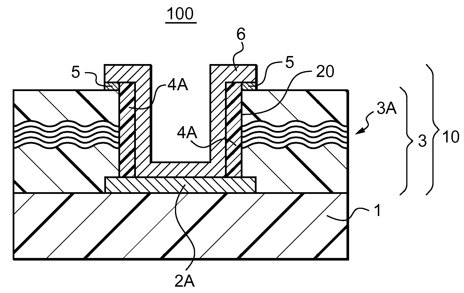
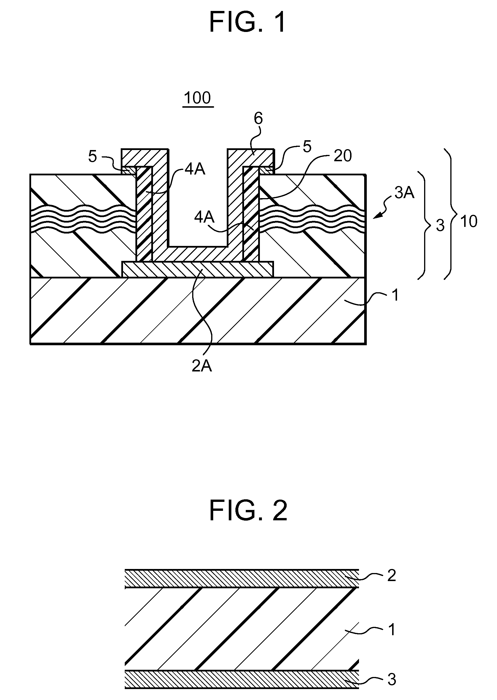
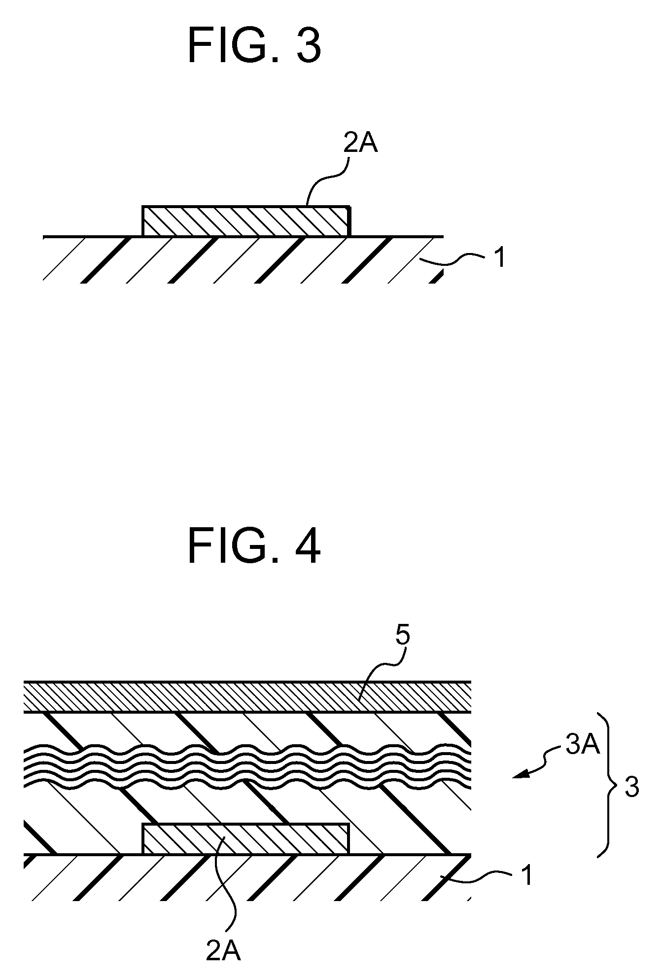
[0018]A printed wiring board according to the present invention comprises a base substrate, a land conductor layer, an insulating layer, a via conductor layer, and a block layer. The land conductor layer is provided on the base substrate at least in part thereof. The insulating layer is provided on the base substrate and the land conductor layer, has a via hole reaching the land conductor layer, and contains glass fibers. The via conductor layer covers a surface of the via hole and a surface of the insulating layer at least in the vicinity of an opening of the via hole and is connected to the land conductor layer. The block layer is provided between the surface of the via hole and the via conductor layer for preventing migration to the via conductor layer through the glass fibers inside the insulating layer. The block layer covers the inner wall of the insulating layer at least over a range from the uppermost end to the lowermost end where the glass fibers inside the insulating laye...


PUM

PropertyMeasurementUnit
thicknessaaaaaaaaaa
thicknessaaaaaaaaaa
hole diameteraaaaaaaaaa

Abstract

A printed wiring board has a via land, a glass epoxy resin layer, a via conductor, and a block layer. The via land is formed on a core layer. The glass epoxy resin layer is formed on the core layer and the via land. The via conductor is formed on the via land. The block layer is formed on the via land, between the via conductor and the glass epoxy resin layer.

Description

FIELD OF THE INVENTION[0001]The present invention relates to a printed wiring board and its manufacturing method and, more specifically, relates to a printed wiring board having a base substrate such as a core layer and a method of manufacturing such a printed wiring board.BACKGROUND OF THE INVENTION [0002]In recent years, attention has been given to printed wiring boards to build-up printed wiring boards that are capable of increasing packaging density. As shown in FIG. 20, a build-up wiring board has a structure in which a plurality of build-up layers 600 are stacked on a core layer 500 serving as a base, and a plurality of vias 700 are formed in the build-up layers 600 for establishing electrical connection between the layers.[0003]For realizing high-density packaging, it is necessary to shorten a distance (pitch) between the vias. However, if the pitch between the vias is small, a short is caused due to migration or back plating. The migration is a phenomenon that when metal is ...

Claims


Application Information

Patent Timeline
Patent Type & Authority Applications(United States)
IPC IPC(8): H01R12/04H05K3/02H05K1/03H05K3/42H05K3/46
CPCH05K1/0366H05K3/421H05K3/4644Y10T29/49155H05K2201/0769H05K2201/09509H05K2201/09581H05K2201/029H05K3/46
Inventor MORI, HIROYUKIYAMANAKA, KIMIHIROKODAMA, YASUSHI
Owner IBM CORP
Why Eureka
Try Eureka