TFT array substrate and manufacturing method thereof

a technology of array substrate and manufacturing method, which is applied in the direction of instruments, semiconductor devices, electrical apparatus, etc., can solve the problems of difficult and expensive development process, difficult to increase yield, and difficult to achieve the effect of improving yield

Active Publication Date: 2008-07-10
BEIJING BOE OPTOELECTRONCIS TECH CO LTD +1
View PDF8 Cites 37 Cited by
  • Summary
  • Abstract
  • Description
  • Claims
  • Application Information

AI Technical Summary

Problems solved by technology

However, since the process employs a slit mask, which requires a strict manufacturing accuracy for the photolithography, difficulty and cost for developing the process are increased remarkably and it is hard to increase the yield.

Method used


Image

  • TFT array substrate and manufacturing method thereof
  • TFT array substrate and manufacturing method thereof
  • TFT array substrate and manufacturing method thereof

Examples


Embodiment Construction

[0031]Exemplary embodiments of the present invention will be described hereinafter with reference to the accompanying drawings. However, the present invention can be realized in different ways and should not be limited to the embodiments set forth hereinafter. In the description, when a layer or a element is referred to as being “on” or “connected to” another layer or element, this layer or element can be directly on or directly connected to the other layer or element, or an intervening layer may also be present therebetween.

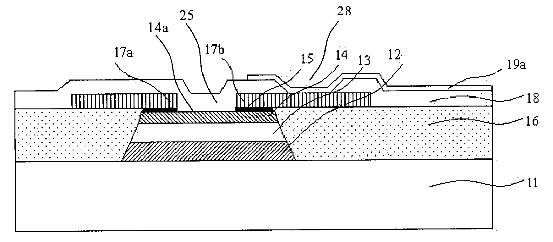
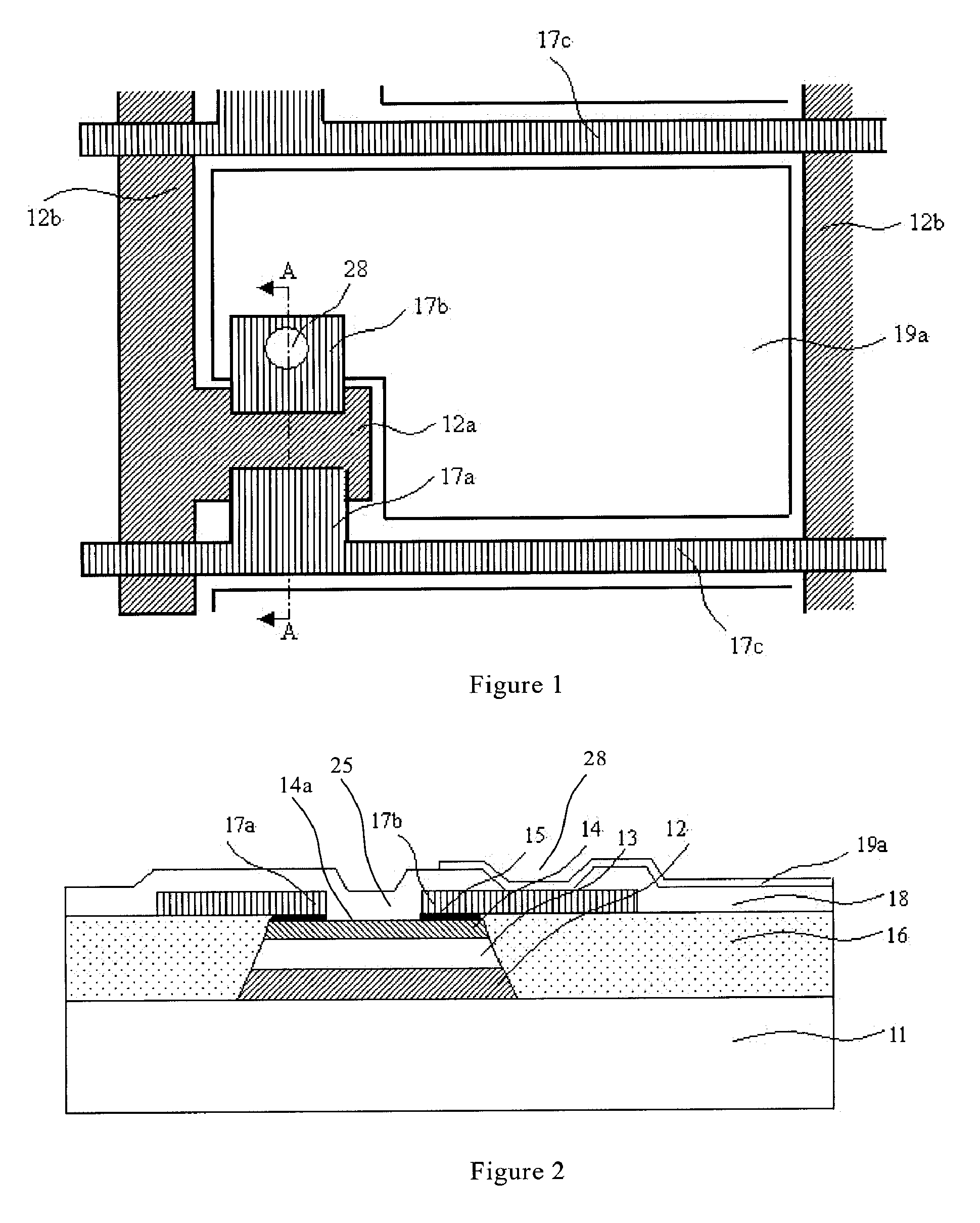
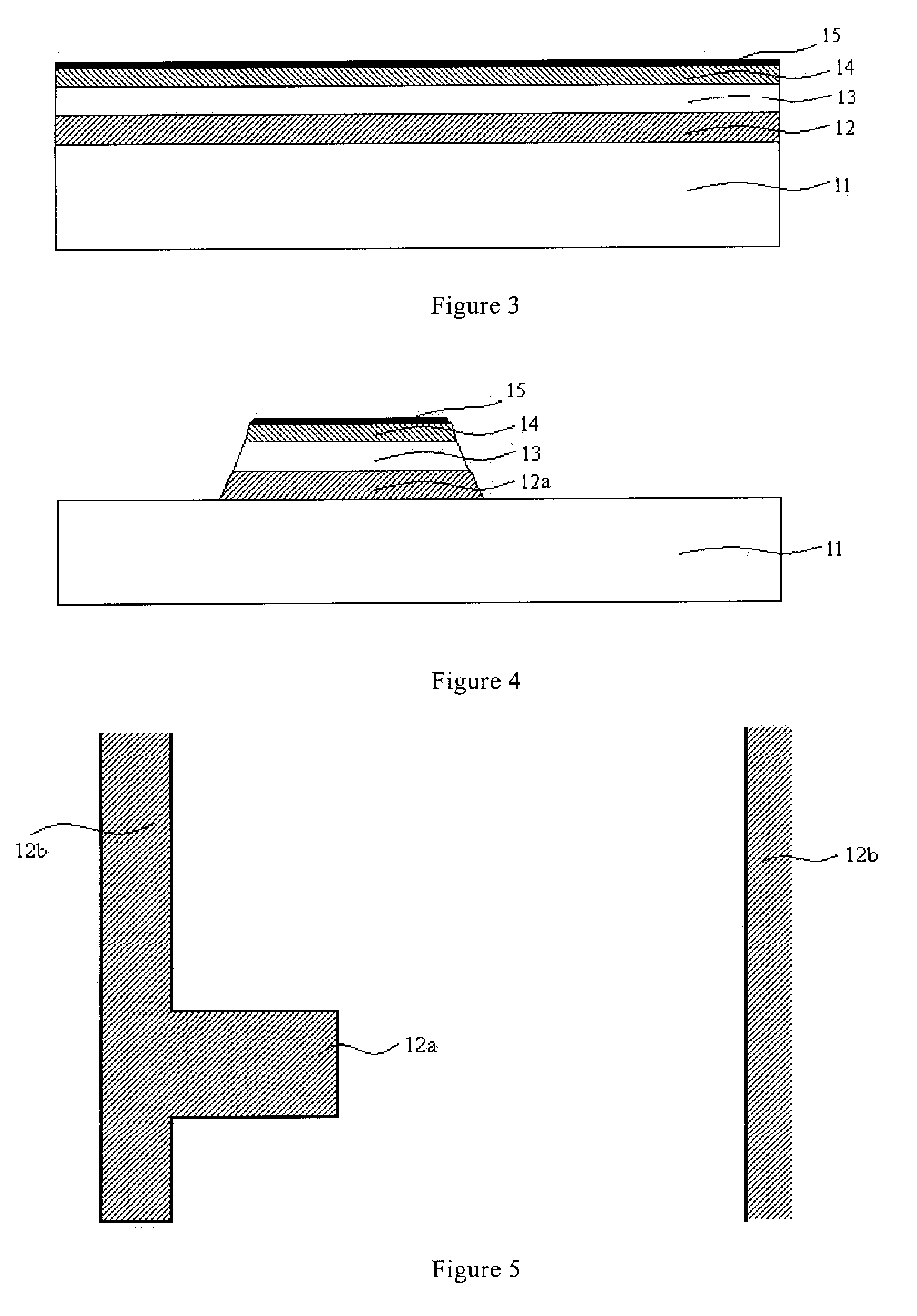
[0032]FIG. 1 is a plan view of a pixel area on a TFT array substrate according to an embodiment of the present invention, and FIG. 2 is a cross-sectional view taken along the line A-A in FIG. 1.

[0033]As shown in FIG. 1, for example, the TFT array substrate according to the embodiment of the present invention comprises a plurality of gate lines 12b extending parallel to each other and a plurality of data lines 17c extending parallel to each other. These gate line...


PUM


Abstract

A TFT array substrate and a manufacturing method thereof, where the TFT array substrate includes a substrate; a gate line and a gate electrode integrated therewith, which are covered by a gate insulating layer, a semiconductor layer, and a ohmic contact layer sequentially. An insulating layer is formed on the resulting substrate and on both sides of the gate line and the gate electrode, the gate insulating layer, the semiconductor layer, and the ohmic contact layer. A trench is then formed in the ohmic contact layer to divide the ohmic contact layer over the semiconductor layer. A data line and first and second source/drain electrodes are then formed on the insulating layer and the ohmic contact layer.

Description

BACKGROUND OF THE INVENTION[0001]The present invention relates to a TFT array substrate of a thin film transistor liquid crystal display (TFT LCD) and a manufacturing method thereof.[0002]In order to effectively reduce the manufacturing cost of a TFT LCD and improve its yield, the manufacturing process of the newly developed active driven TFT array substrate has been gradually simplified, for example, from a seven- or a six-photolithography process at the beginning to a current widely employed five-photolithography process. Recently, a four-photolithography process based on a slit photolithography process (a gray tone photolithography process) is applied in the field of TFT LCD manufacturing, the core step of which is to replace the second photolithography (an active layer photolithography) and the third photolithography (a source / drain metal layer photolithography) of the conventional five-photolithography process with one slit photolithography process. The detailed procedure of th...

Claims


Application Information

Patent Timeline
Patent Type & Authority Applications(United States)
IPC IPC(8): H01L29/04H01L21/336
CPCH01L27/1214H01L27/1248H01L27/1288H01L29/66765G02F1/136
Inventor WANG, ZHANGTAOQIU, HAIJUNMIN, TAE YUPRIM, SEUNG MOO
Owner BEIJING BOE OPTOELECTRONCIS TECH CO LTD
Why Eureka
Try Eureka