

Photovoltaic device
a photovoltaic device and photoelectric efficiency technology, applied in the field of semiconductor devices, can solve the problems of limited photoelectric efficiency of conventional photovoltaic devices b>100/b>, pollution and other problems, and achieve the effect of high photoelectric efficiency
- Summary
- Abstract
- Description
- Claims
- Application Information
AI Technical Summary
Benefits of technology
Problems solved by technology
Method used
Image

Examples
first embodiment
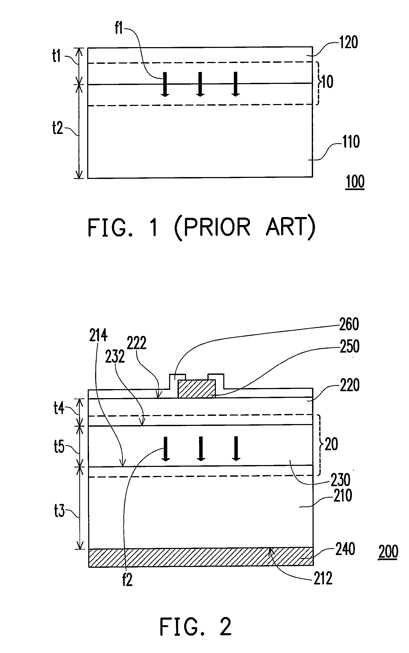
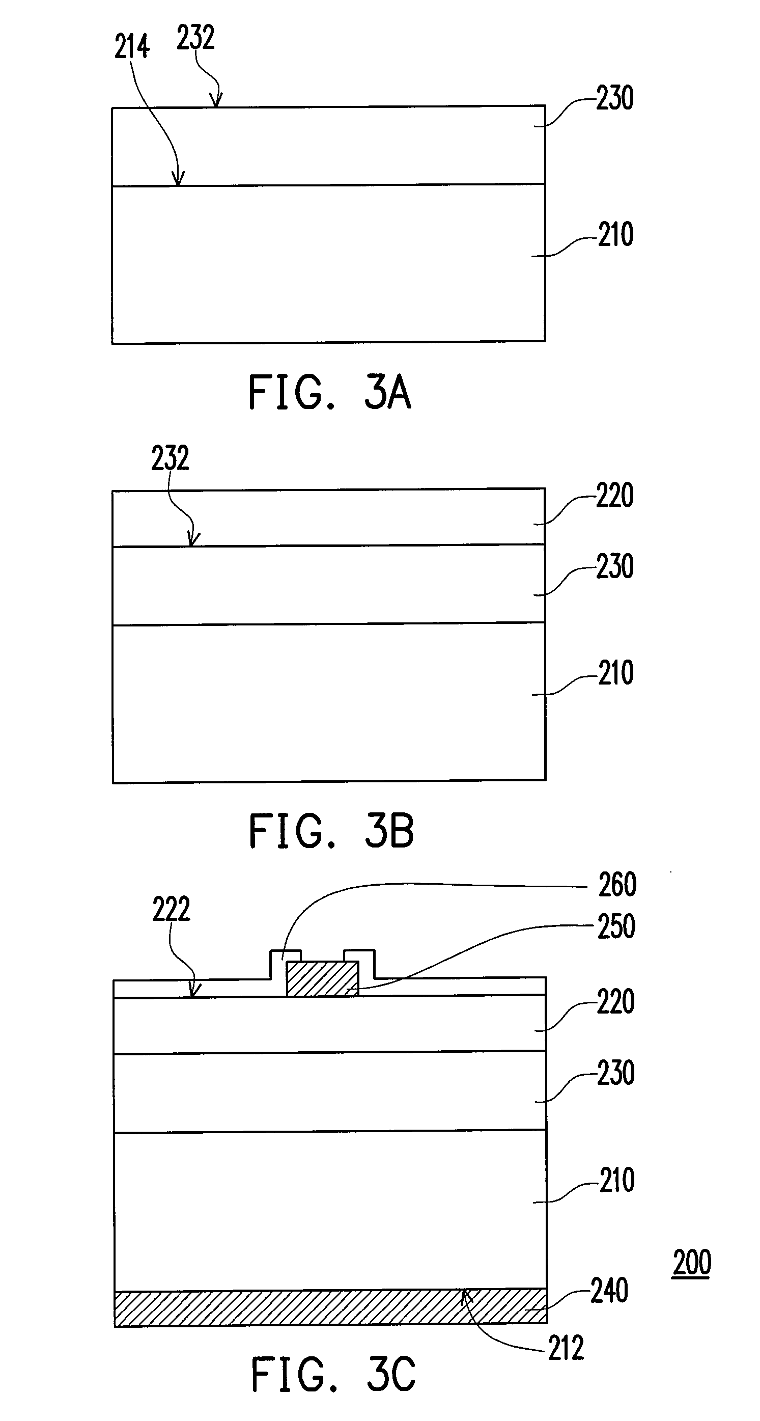
[0050]FIG. 2 demonstrates a schematic cross section view of a photovoltaic device according to a first embodiment of the present invention. Referring to FIG. 2, the photovoltaic device 200 includes a first type doped single crystal silicon substrate 210, a second type doped silicon layer 220, an intrinsic silicon layer 230, a first metal electrode layer 240, and a second metal electrode layer 250. The intrinsic silicon layer 230 is disposed between the first type doped single crystal silicon substrate 210 and the second type doped silicon layer 220. The thickness t5 of the intrinsic silicon layer is between 10 μm and 100 μm. The first metal electrode layer 240 is disposed on a surface 212 of the first type doped single crystal silicon substrate 210 away from the intrinsic silicon layer 230. The second metal electrode layer 250 is disposed on a surface 222 of the second type doped silicon layer 220 away from the intrinsic silicon layer 230.
[0051]Since the intrinsic silicon layer 230 ...
second embodiment
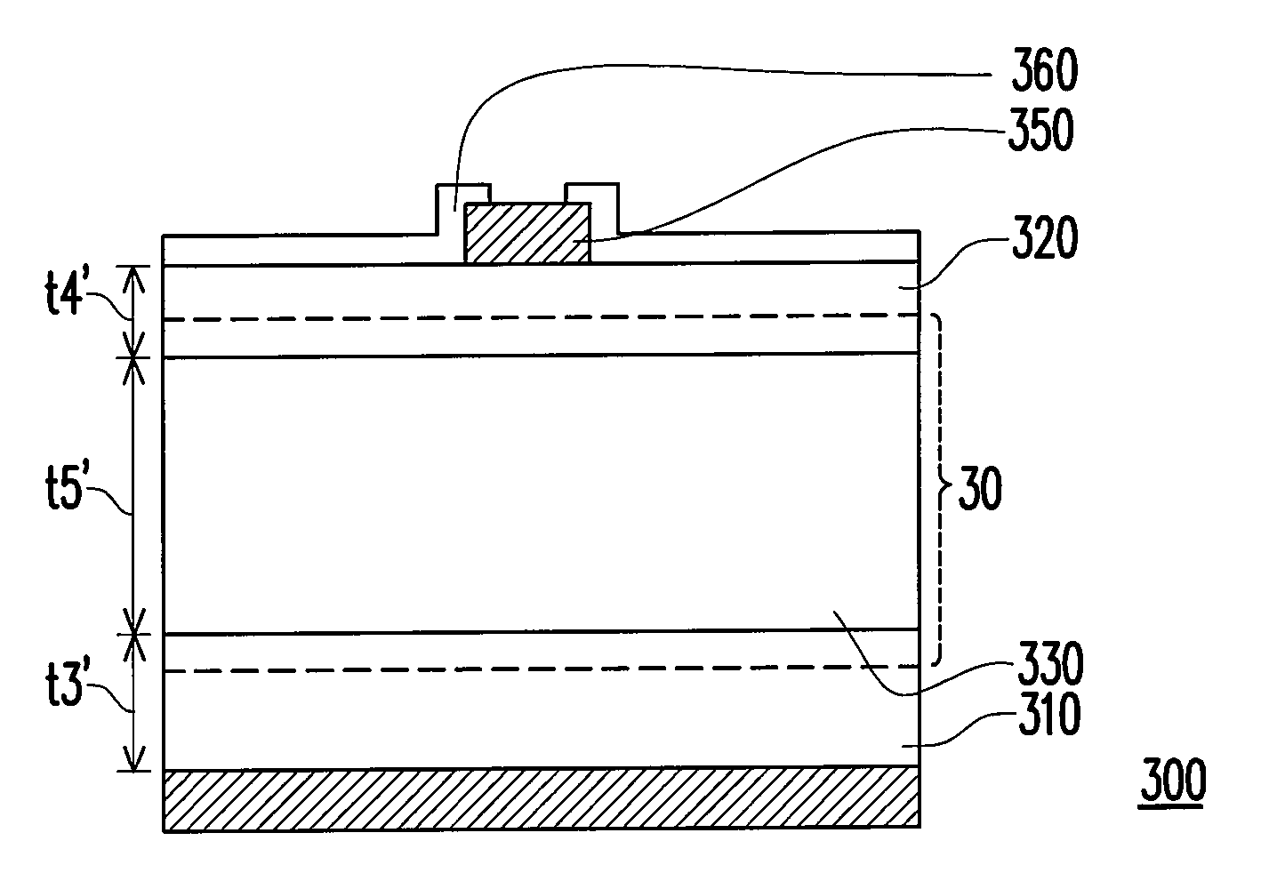
[0063]FIG. 4 demonstrates a schematic cross section view of a photovoltaic device according to a second embodiment of the present invention. Referring to FIG. 4, the photovoltaic device 300 has an intrinsic silicon substrate 330 of which the thickness t5′ is between 50 μm and 200 μm. In the present embodiment, the thickness t3′ of the first type doped silicon layer 310 may be between 0.3 μm and 10 μm, and preferably, the thickness t3′ of the first type doped silicon layer 310 is between 0.3 μm and 1 μm. The thickness t4′ of the second type doped silicon layer 320 may be between 0.03 μm and 1 μm, and preferably, the thickness t4′ of the second type doped silicon layer 320 may be between 0.05 μm and 0.5 μm.
[0064]It should be noted that external sunlight passes through silicon layer 320 and then is absorbed and electron-hole pairs are generated in the depletion region 30, so thinner thickness t4′ of silicon layer 320 has better efficiency. However, the internal resistance becomes highe...
third embodiment
[0068]FIG. 6 demonstrates a schematic cross section view of a photovoltaic device according to a third embodiment of the present invention. Referring to FIG. 6, the photovoltaic device 400 includes an N-type doped silicon layer 410, a first electrode layer 420, an intrinsic silicon layer 430, and a second electrode layer 440. The first electrode layer 420 has a conductive layer 422 (for example, platinum), and the work function of the conductive layer 422 is higher than 5.5 eV. The intrinsic silicon layer 430 is disposed between the N-type doped silicon layer 410 and the first electrode layer 420, and the conductive layer 422 is in direct contact with the intrinsic silicon layer 430. The second electrode layer 440 is disposed on a surface 412 of the N-type doped silicon layer 410 away from the intrinsic silicon layer 430.
[0069]In the present embodiment, since the conductive layer 422 having work function higher than 5.5 eV is in direct contact with the intrinsic silicon layer 430, t...
PUM
| Property | Measurement | Unit |
|---|---|---|
| thickness | aaaaa | aaaaa |
| thickness | aaaaa | aaaaa |
| thickness | aaaaa | aaaaa |
Abstract
Description
Claims
Application Information