Semiconductor device

a technology of semiconductor devices and semiconductors, applied in the direction of semiconductor devices, semiconductor/solid-state device testing/measurement, semiconductor/solid-state device details, etc., can solve the problem of leakage of confidential and prevent leakage of information regarding semiconductor design and manufacture. , no cost increase of semiconductor devices is caused, the effect of preventing a leakage of information

Inactive Publication Date: 2008-07-17
LONGITUDE SEMICON S A R L
View PDF11 Cites 9 Cited by
  • Summary
  • Abstract
  • Description
  • Claims
  • Application Information

AI Technical Summary

Benefits of technology

[0013]As mentioned above, in case where the semiconductor device is shipped to a customer in a wafer state, it is possible to measure the characteristic checking element. This causes a problem that, by measuring and analyzing the characteristic checking element, confidential matters regarding semiconductor design and manufacture are leaked outside. It is therefore an object of the present invention to prevent, in a semiconductor device shipped in a wafer state, a leak of information regarding semiconductor design and manufacture. For that purpose, the characteristic checking element is broken in an existing process (without requiring an additional process) so that no accurate measurement value is indicated. Thereafter, the semiconductor device is shipped in a wafer state. It is also an object of the present invention to provide a semiconductor device provided with a characteristic checking element, which is capable of preventing a leak of information regarding semiconductor design and manufacture, such as transistor characteristics, by breaking the characteristic checking element.
[0026]The semiconductor device of the present invention has the internal measurement pad additionally disposed inside the semiconductor device. In the process (PAN process) of verifying operations of the semiconductor device in a wafer state, an electric voltage is applied to the internal measurement pad to destroy the function of the characteristic checking element. At the time of shipping, the function of the characteristic checking element is broken. Therefore, the present invention provides an effect that a leak of information regarding semiconductor design and manufacture can be prevented. Further, since the function of the characteristic checking element is destroyed in an existing process, i.e. the process of verifying operations of the semiconductor device, an additional process is not required. Therefore, another effect is obtained that no cost increase of the semiconductor device is caused. According to the present invention, it is possible to provide a semiconductor device capable of destroying a function of a characteristic checking element without requiring a special additional process and preventing a leak of information regarding semiconductor design and manufacture.

Problems solved by technology

This causes a problem that, by measuring and analyzing the characteristic checking element, confidential matters regarding semiconductor design and manufacture are leaked outside.

Method used


Image

  • Semiconductor device
  • Semiconductor device
  • Semiconductor device

Examples


first embodiment

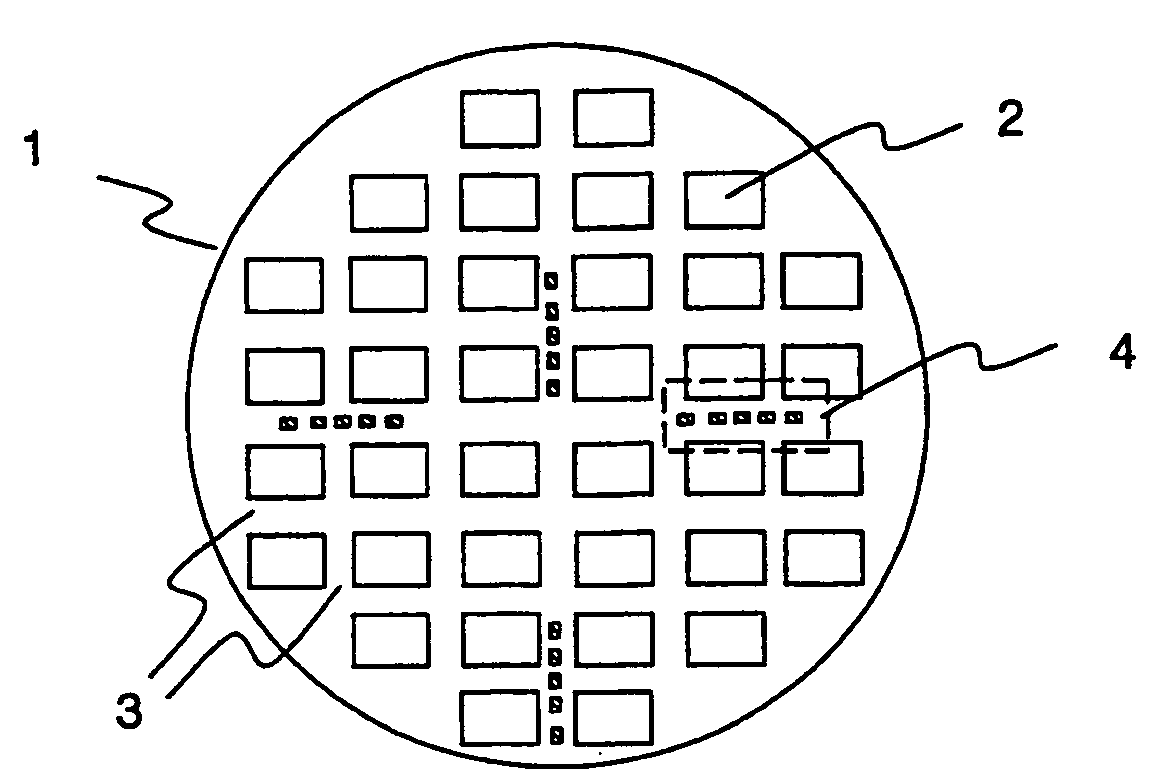
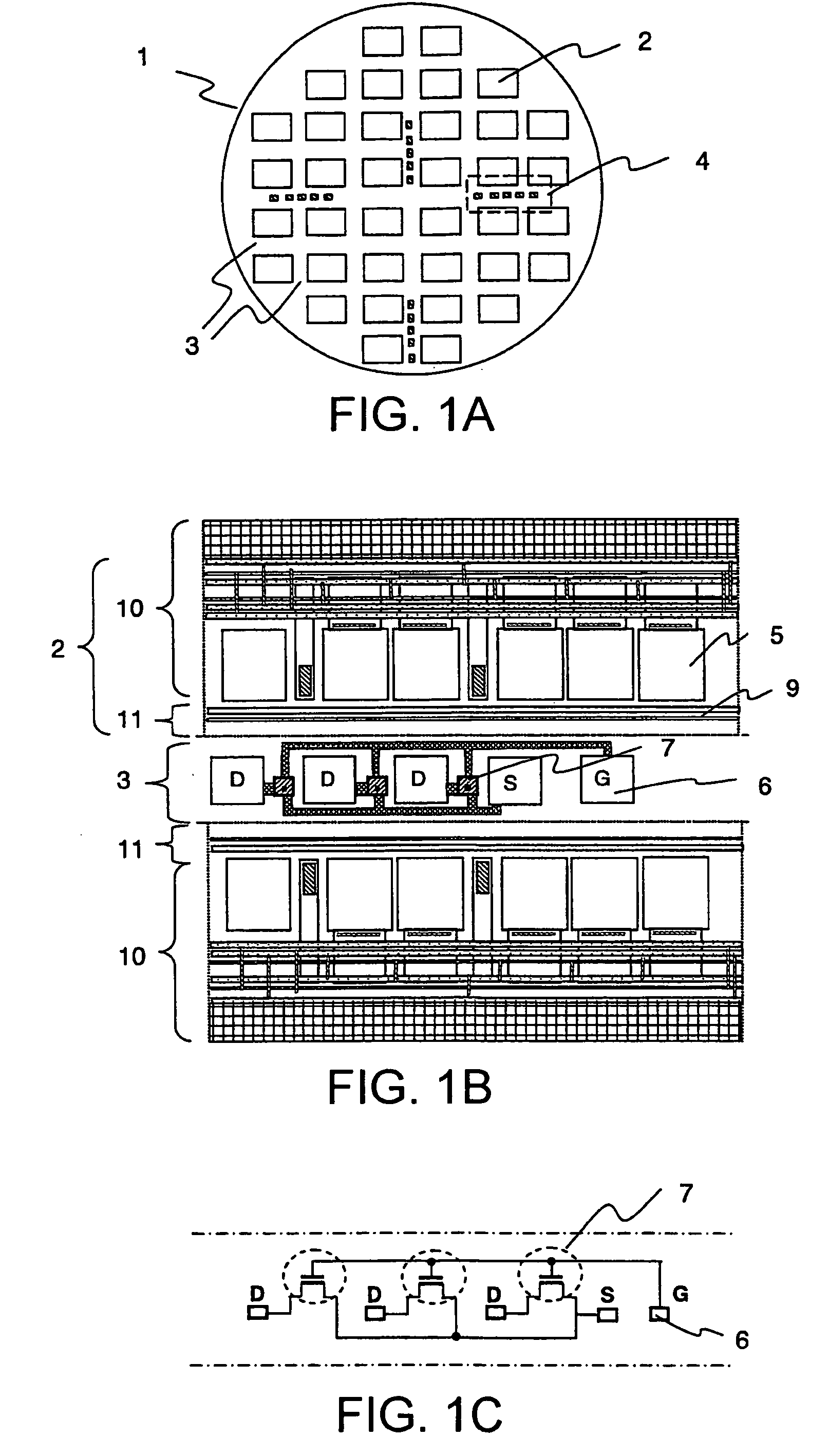
[0050]Referring to FIGS. 2 and 3, a semiconductor device according to a first embodiment of the present invention will be described. As a characteristic checking element of the first embodiment, three checking transistors are shown by way of example. FIGS. 2A, 2B, and 2C show a plan view of a wafer, a view showing a pad arrangement of the characteristic checking element, and a view showing connection of the checking transistors as the characteristic checking element, respectively. FIGS. 3A, 3B, and 3C show a plan view of the wafer, an enlarged plan view of a part of the wafer, and a sectional view of a sub-connection wiring taken along a line A-A′ in FIG. 3B, respectively.

[0051]On a wafer 1, a plurality of semiconductor devices 2 are arranged in a matrix fashion. Each of the semiconductor devices 2 has four sides surrounded by dicing lines 3. The dicing lines 3 for separating and segmenting the wafer 1 into the individual semiconductor devices 2 are formed in vertical and horizontal...
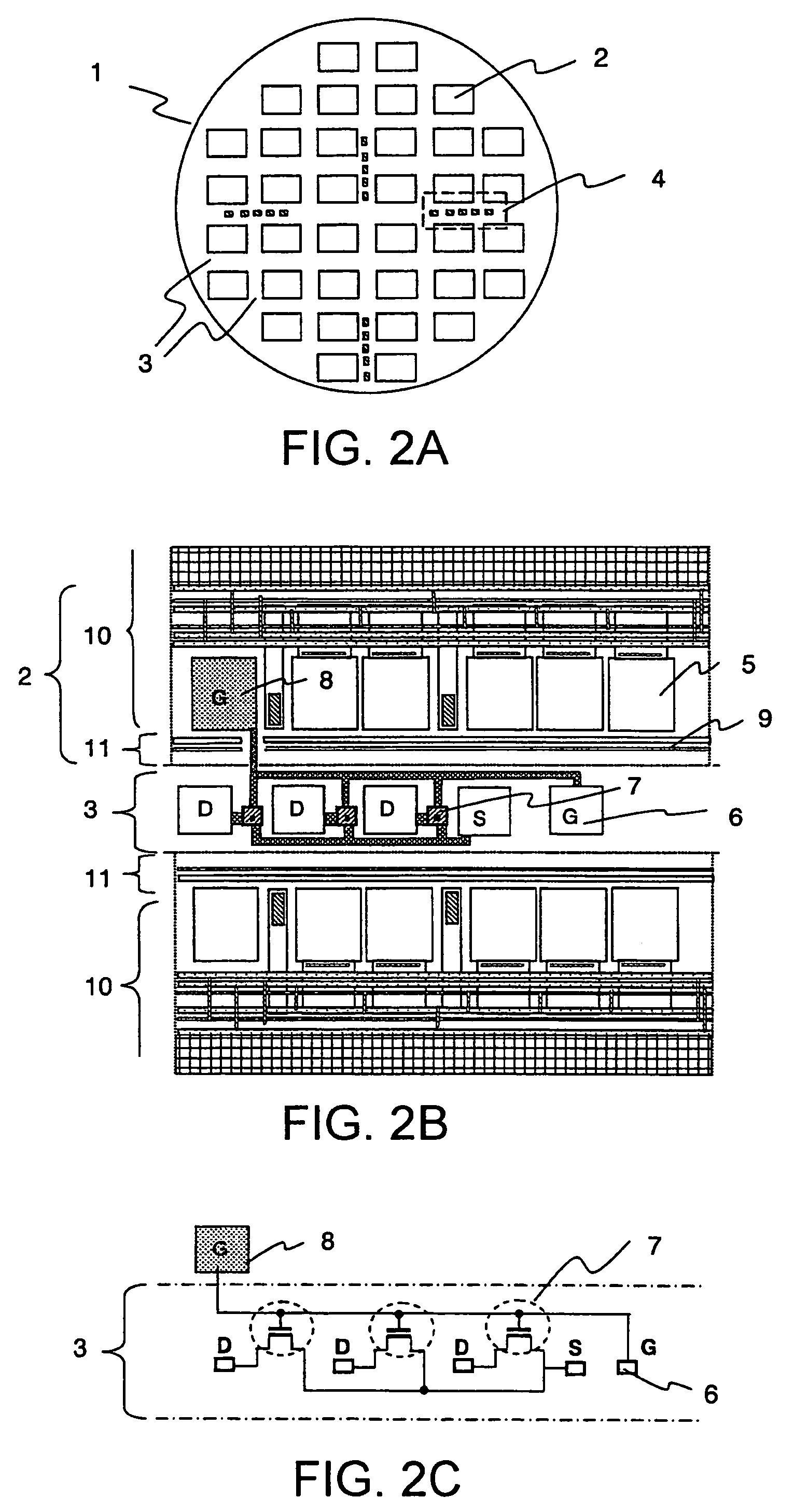
second embodiment

[0059]Referring to FIGS. 4 through 9B, a semiconductor device according to a second embodiment of the present invention will be described. As a characteristic checking element of the second embodiment, checking resistance elements are shown by way of example. It is difficult to break the checking resistance elements merely by applying an electric voltage. Therefore, in this embodiment, the checking resistance elements constituting the characteristic checking element are connected to an easily breakable transistor. FIGS. 4 through 8 are views showing first through fifth examples of circuit connections of the checking resistance elements, respectively. FIGS. 9A and 9B show arrangements of the checking resistance elements.

[0060]FIG. 4 is a view showing the first example of circuit connection in case where the characteristic checking element comprises the checking resistance elements. It is difficult to break the checking resistance elements merely by applying an electric voltage. There...

third embodiment

[0069]Referring to FIGS. 10A, 10B, 11A, and 11B, a semiconductor device according to a third embodiment of the present invention will be described. This embodiment shows connection between an internal measurement pad and a characteristic checking element in a wafer state. As the characteristic checking element, three checking transistors are shown by way of example. FIG. 10A is a plan view of a wafer and FIG. 10B is a connection diagram of a reticle for use in a photolithography process. FIGS. 11A and 11B show an embodiment in which the characteristic checking elements are connected to one another by the dicing line. FIG. 11A is a plan view of a wafer and FIG. 11B is a connection diagram of a reticle for use in the photolithography process.

[0070]Description will be made about connection of the characteristic checking elements 4 on the reticle 13 in FIG. 10B. On the reticle 13, the semiconductor devices 2 are disposed, nine in total, in three (top, middle, and bottom) horizontal rows...


PUM


Abstract

A transistor of a characteristic checking element has a gate electrode connected to a measurement pad disposed in a dicing line and to an internal measurement pad disposed inside a semiconductor device. In a P / W process, a gate insulating film of the transistor is broken by an electric voltage applied via the internal measurement pad. Since the gate insulating film of the transistor is broken, a new current path is formed. Thus, measurement of accurate characteristics of the characteristic checking element is inhibited.

Description

[0001]This application is based upon and claims the benefit of priority from prior Japanese patent application JP 2007-004349, filed on Jan. 12, 2007, the disclosure of which is incorporated herein by reference in its entirety.BACKGROUND OF THE INVENTION[0002]This invention relates to a semiconductor device and, in particular, to a semiconductor device provided with a characteristic checking element for checking electric characteristics.[0003]A semiconductor device is produced through a number of manufacturing processes and shipped to a customer. As a front-end process (diffusion process) of the semiconductor device, a deposition process, a photolithography process, and an impurity diffusion process are repeatedly executed on a semiconductor substrate (sub). Through such a number of processes, a wafer with a plurality of semiconductor devices formed thereon is completed. The wafer thus completed is subjected to a pellet / wafer test process (hereinbelow, will be called a P / W process) ...

Claims


Application Information

Patent Timeline
Patent Type & Authority Applications(United States)
IPC IPC(8): H01L23/58
CPCH01L22/34H01L2924/0002H01L2924/00
Inventor YAMAGAMI, MINORUNAGAMINE, HISAYUKI
Owner LONGITUDE SEMICON S A R L
Why Eureka
Try Eureka