Batch-test system with a chip tray

Active Publication Date: 2008-07-17
VISERA TECH CO LTD
View PDF14 Cites 20 Cited by
  • Summary
  • Abstract
  • Description
  • Claims
  • Application Information

AI Technical Summary

Problems solved by technology

In a conventional chip test procedure, a specific chip test apparatus is required and the chip test apparatus cannot be shared to test different chips, thus, the test cost increases.
Moreover, the present chip test apparatus cannot test a l

Method used


Image

  • Batch-test system with a chip tray
  • Batch-test system with a chip tray
  • Batch-test system with a chip tray

Examples


Embodiment Construction

[0020]The following description is of the best-contemplated mode of carrying out the invention. This description is made for the purpose of illustrating the general principles of the invention and should not be taken in a limiting sense. The scope of the invention is best determined by reference to the appended claims.

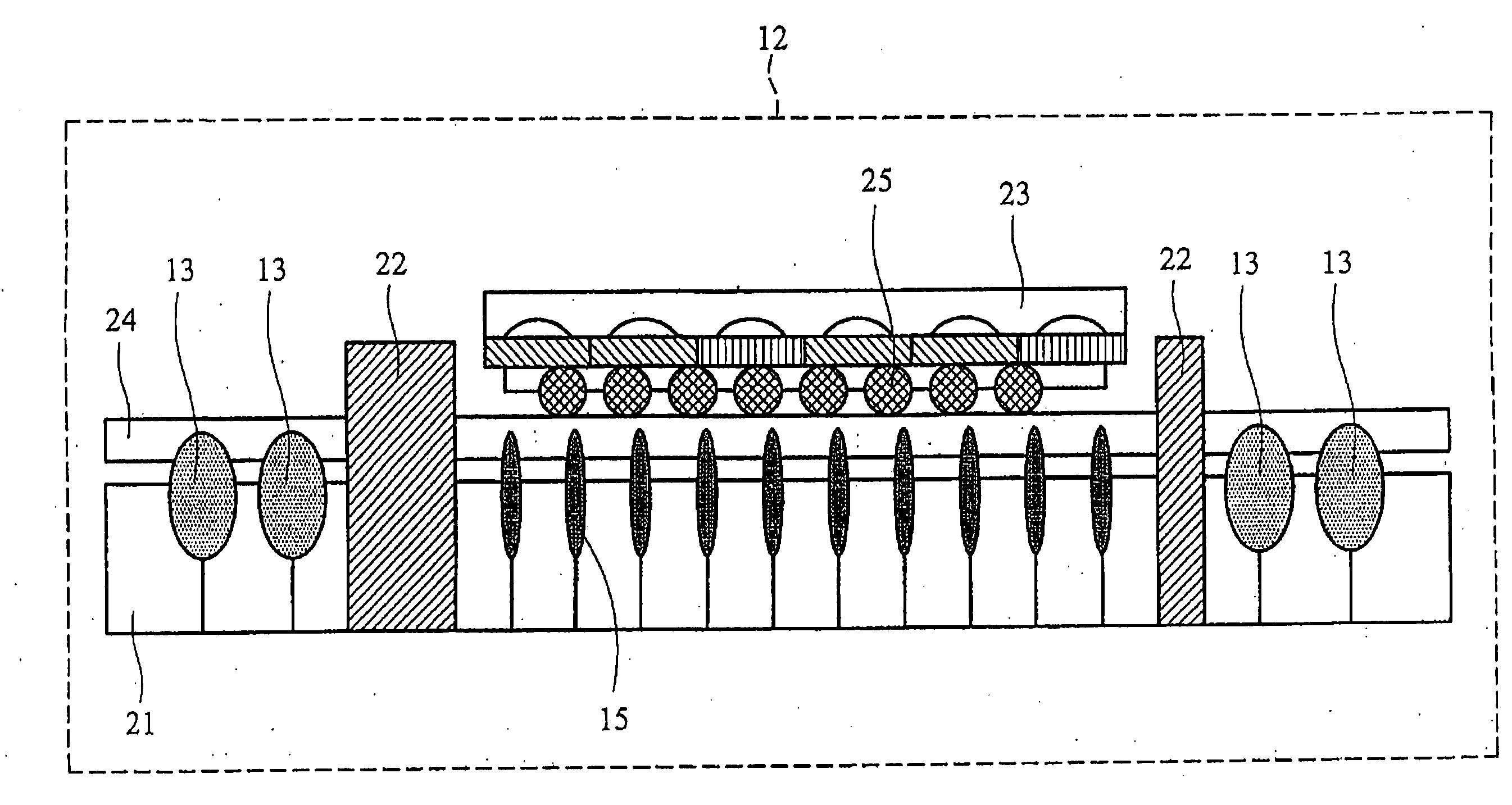
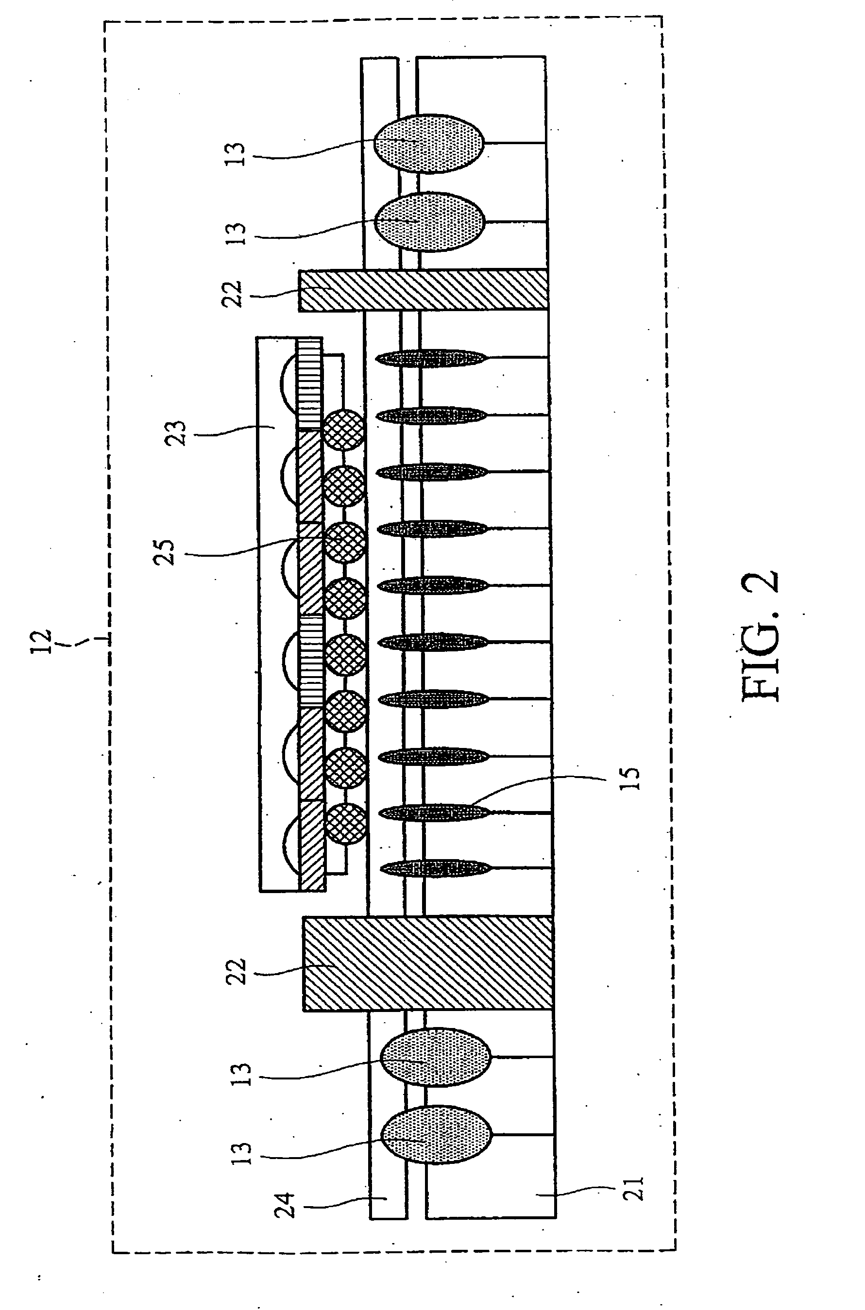
[0021]Probe cards have been used for testing electrical properties and circuit functions of semiconductor chips formed on a semiconductor wafer. Typically, testing is conducted in on semiconductor chips still in wafer form. The probe card is pressed against the wafer so that probes of the probe card contact corresponding electrode pads on the semiconductor chip. The probes of the probe card and an interconnection structure on the probe card thus provide connection between the semiconductor chip and a testing apparatus to which the probe card is connected.

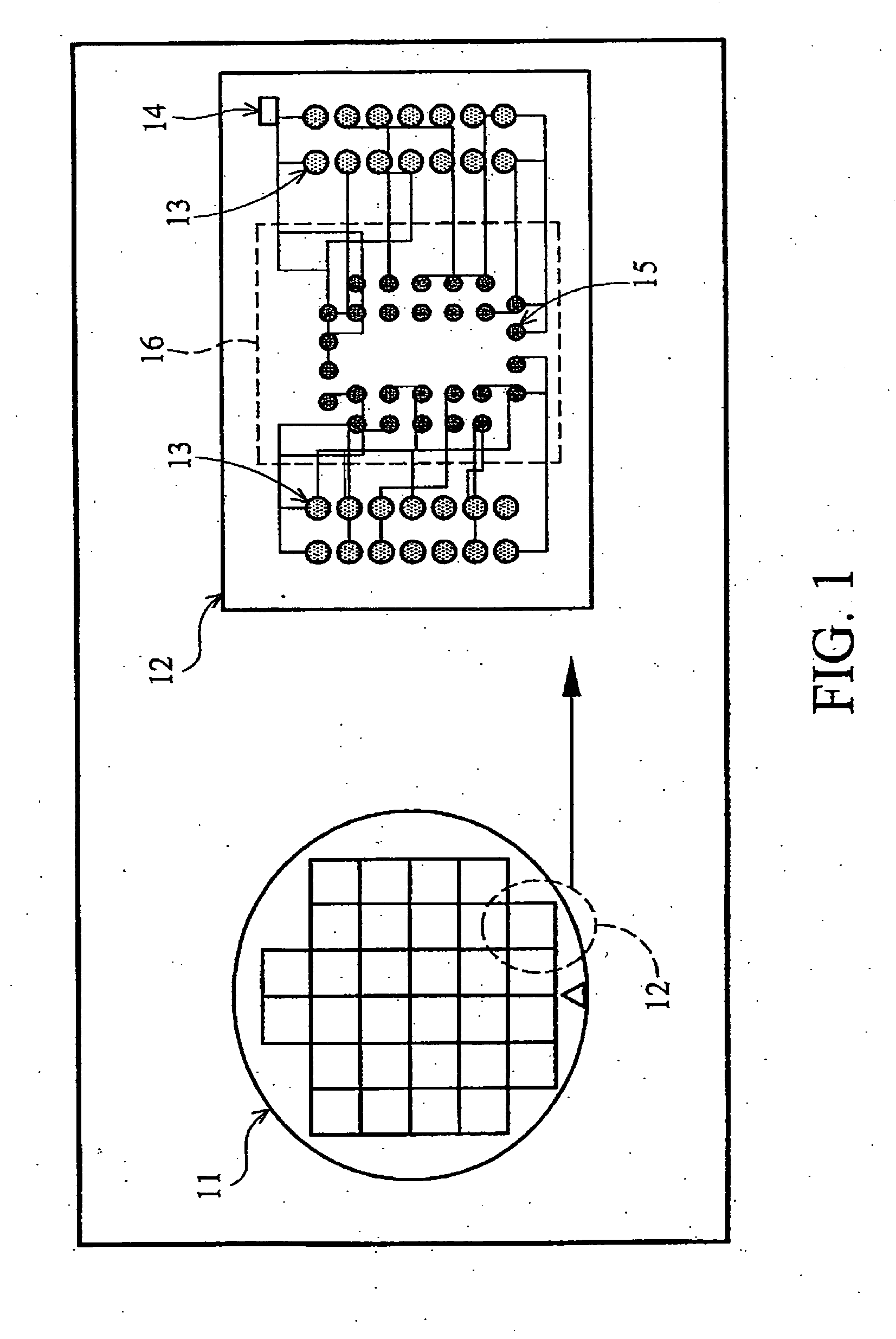
[0022]FIG. 1 is a schematic diagram showing an embodiment of a chip tray of the invention. The chip tray 11 comprise...


PUM


Abstract

A chip test system including a probe card, a chip tray and a cover plate fastened on the chip tray. The chip tray comprises a socket, a chip contact area, an extension contact area, and an alignment contact point. The socket loads the testing chip and is customized for the tested chip. The chip contact area has a plurality of chip contact points to electrically contact the chip. The extension contact area has a plurality of extension contact points corresponding to the chip contact points to direct test signals into the chip and direct feedback signals out of the chip. The alignment point provides an alignment location for the probe card during the chip test.

Description

BACKGROUND OF THE INVENTION[0001]1. Field of the Invention[0002]The invention relates to a test system, and more particularly to a batch-test system with a chip tray.[0003]2. Description of the Related Art[0004]Recently, there a need for more efficient semiconductor device testing processes has arisen. A semiconductor device is generally subject to a wafer test and a chip test before it is shipped to a user. The wafer test is performed in a wafer state, while the chip test is performed in a chip state after the wafer is diced, assembled and packaged. The wafer test and chip test are performed in order to prevent possible inflow of defective chips in an assembly process, i.e., in order to best reject possible defective chips in a chip state.[0005]In a conventional chip test procedure, a specific chip test apparatus is required and the chip test apparatus cannot be shared to test different chips, thus, the test cost increases. Moreover, the present chip test apparatus cannot test a la...

Claims


Application Information

Patent Timeline
IPC IPC(8): G01R31/26
CPCG01R31/2834G01R31/2886H01L24/73H01L2224/48091H01L2224/73253H01L2924/00014
Inventor LU, SHENG-FENGHSIAO, YU-KUN
Owner VISERA TECH CO LTD
Why Eureka
Try Eureka