
Solid-state imaging device and imaging apparatus

a solid-state imaging and imaging apparatus technology, applied in the direction of solid-state device signal generators, picture signal generators, television systems, etc., can solve the problem of not always being able to obtain an addition image of high resolution, and achieve the effect of preventing resolution from lowering or reducing the possibility of resolution lowering, and sometimes lowering resolution

Active Publication Date: 2008-07-17
SONY CORP
View PDF13 Cites 75 Cited by
  • Summary
  • Abstract
  • Description
  • Claims
  • Application Information

AI Technical Summary

Benefits of technology

[0010]Since a CMOS imaging sensor converts a pixel signal into an electric signal per pixel, such addition processing function can be easily incorporated therein. The solid-state imaging device disclosed in the above-mentioned patent document also adopts this addition processing system.
[0012]The present invention is made in view of the above circumstances, and provides a mechanism capable of obtaining an addition image with high resolution.
[0016]If pixels are provided with color filters for generating color images, the addition spatial position adjusting unit controls the selection operation for selecting the spatial positions of a plurality of pixels to be processed by the comparator so that the pixels having the same color are added, and controls the ratio of the weight value during the addition so that the spatial positions of each pixel are arranged at equal intervals.
[0017]If the spatial position of each pixel after the addition is adjusted by setting an appropriate weight value, the pixel positions after the addition can be arranged at equal intervals in the optimum state. As a result, it is possible to certainly prevent the resolution from lowering or decrease the possibility of resolution lowering, whereas the resolution is sometimes lowered if images are added by the simple addition processing.

Problems solved by technology

However, by performing simple addition processing which makes coefficients of addition object pixels uniform, it is not always possible to obtain an addition image of high resolution due to a relation of spatial positions of pixels after the addition.

Method used


Image

  • Solid-state imaging device and imaging apparatus
  • Solid-state imaging device and imaging apparatus
  • Solid-state imaging device and imaging apparatus

Examples


first embodiment

[Resolution Improving Method for Addition Image: First Embodiment]

[0255]FIGS. 9 to 11 are diagrams illustrating an example of a first embodiment of a method for solving the lowering of resolution in the digital addition processing in the vertical direction by the counter 254 and in the digital addition processing in the horizontal direction by the digital arithmetic unit 29.

[0256]FIGS. 9 and 10 are timing charts illustrating weighted addition processing with respect to the vertical direction, performed in parallel with the A / D conversion processing, in a resolution improving method of the first embodiment. For simplicity of the description, the offset component of the column A / D circuit is ignored. FIG. 11 is a diagram showing an effect when the count clock switch 516 is operated in the resolution improving method of the first embodiment.

[0257]Examples showing in FIGS. 9 and 10 are the addition processing for two pixels, and a weighted ratio between the two pixels is set to 1 to 2 (...

second embodiment

[The Resolution Improving Method for the Addition Image: Second Embodiment]

[0339]FIGS. 18 to 21 are diagrams illustrating the second embodiment of the method for solving the resolution degradation problem in the digital addition processing in the vertical direction by the counter 254 and the digital addition processing in the horizontal direction by the digital arithmetic unit 29.

[0340]FIGS. 18A to 18C are diagrams illustrating a disadvantage of the single-slope integration A / D conversion system. More particularly, the diagrams explain an influence exerted to the A / D conversion performance, particularly to the conversion processing speed, by the comparison processing period in which the analog pixel signal voltage Vx is compared with the reference signal Vslop used for the digital data conversion, and also illustrating an example of a method for shortening the comparison processing period.

[0341]FIG. 19 is a timing chart for illustrating the addition processing with respect to the ve...

third embodiment

[Resolution Improving Method for Addition Image: Third Embodiment]

[0402]FIG. 20 is the diagram illustrating the third embodiment of the method for solving degradation of the resolution in the digital addition processing in the vertical direction by the counter 254 and the digital addition processing in the horizontal direction by the digital arithmetic unit 29.

[0403]In the third embodiment, it is not the case where the weighted addition processing for the two rows and two columns but the case where the weighted addition processing for three rows and three columns. The weighted addition processing for three columns in the column direction is not indispensable.

[0404]When the addition processing performed on three pixels, for example, the weight for three pixels may be different from each other or the weight for only one pixel is different from that for other two pixels. In the latter case, for example, the relation between them is set in a ratio of 1 to n to 1 (n is a value more than ...


PUM


Abstract

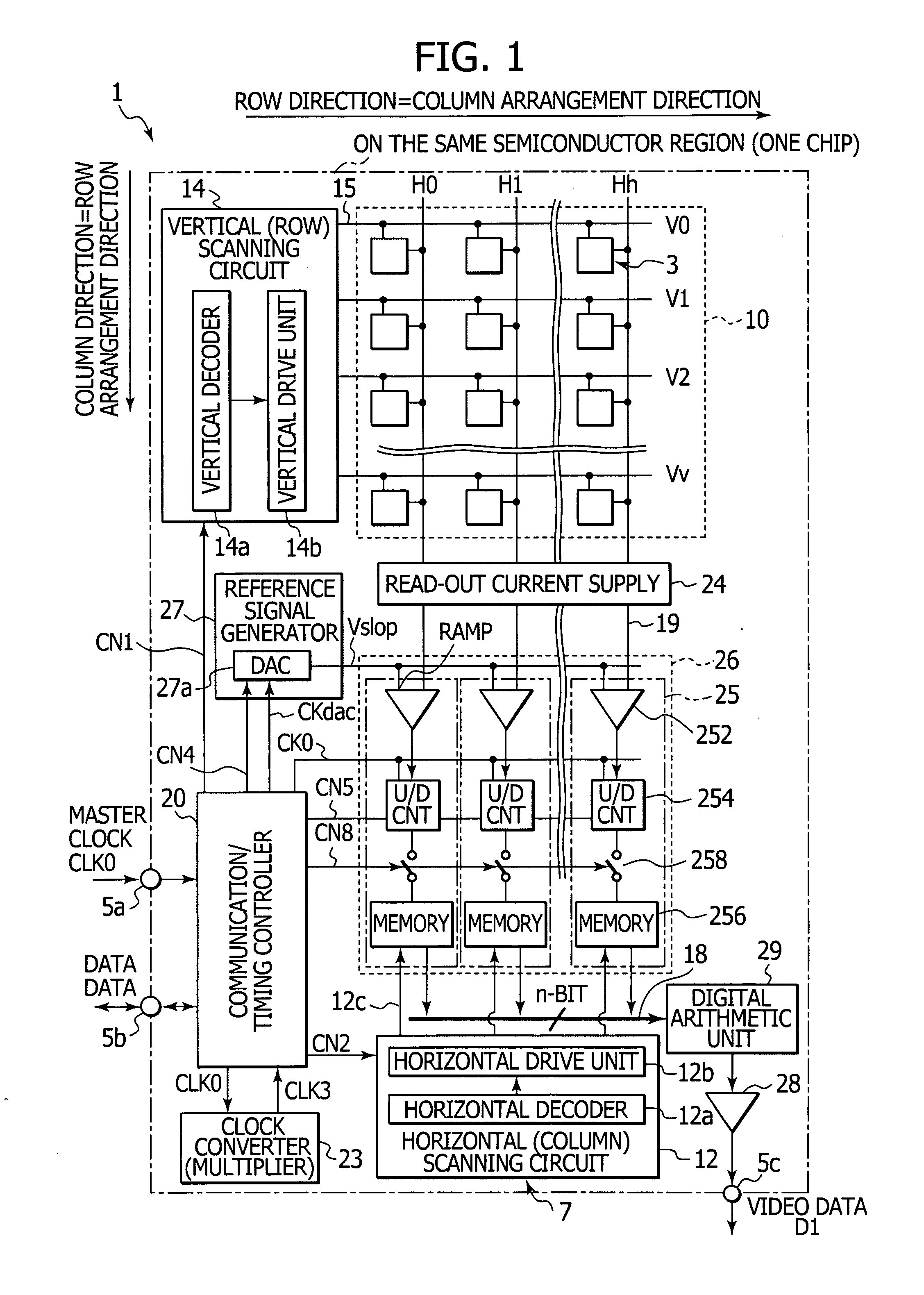
There is provided a solid-state imaging device, which includes: a comparator for sequentially comparing a predetermined level of an analog pixel signal obtained from a plurality of pixels with a reference signal which is gradually changed and used for converting the predetermined level into digital data; a counter for performing a count processing in parallel with a comparison processing for the predetermined level in the comparator, and holding a count value at a time of completing the comparison processing to obtain digital data indicative of a value obtained by adding the plurality of pixel signals; and an addition spatial position adjusting unit for controlling a selection operation for selecting spatial positions of the plurality of pixels to be processed in the comparator and a ratio of a weight value during the addition to adjust spatial positions of pixels after addition.

Description

BACKGROUND OF THE INVENTION[0001]1. Field of the Invention[0002]The present invention relates to a solid-state imaging device and an imaging apparatus, which are examples of a semiconductor device for detecting physical quantity distribution. More specifically, the invention relates to a mechanism including a plurality of arranged unit elements having sensitivity to electromagnetic waves input such as light or radiations from the outside, which reads out a physical quantity distribution converted into an electric signal by the unit elements as an analog electronic signal, converts the analog electronic signal into digital data, and outputs the digital data to the outside.[0003]2. Description of Related Art[0004]In recent years, as an example of solid-state imaging device, a Metal Oxide Semiconductor (MOS) imaging sensor and a Complementary Metal-Oxide Semiconductor (CMOS) imaging sensor have been attracted attention, which are able to solve various disadvantages of a Charge Coupled ...

Claims


Application Information

Patent Timeline
IPC IPC(8): H04N5/225
CPCH04N5/347H04N5/3537H04N9/045H04N5/3575H04N5/35509H04N25/46H04N25/534H04N25/571H04N25/616
Inventor MATSUMOTO, SHIZUNORIHISAMATSU, YASUAKI
Owner SONY CORP
Features
  • Generate Ideas
  • Intellectual Property
  • Life Sciences
  • Materials
  • Tech Scout
  • Unparalleled Data Quality
  • Higher Quality Content
  • 60% Fewer Hallucinations
Learn More