LED array and method for fabricating same

a technology of led arrays and led arrays, which is applied in the field of interconnected light emitting diode arrays, can solve the problems of reducing the efficiency of the array, complex circuitry needed to connect the arrays, and difficulty in providing the necessary electrical connections to power the led arrays

Active Publication Date: 2008-07-17
CREELED INC
View PDF108 Cites 191 Cited by
  • Summary
  • Abstract
  • Description
  • Claims
  • Application Information

AI Technical Summary

Benefits of technology

[0010]One embodiment of an emitter array according to the present invention comprises a submount having a plurality of edges, with input and output terminals and a plurality of attach pads on the submount. A plurality of solid state emitters is included, with at least one of each mounted on and electrically connected to each of the attach pads. The attach pads cover more of the submount than ...

Problems solved by technology

Providing the necessary electrical connections to power the LED arrays can be challenging.
As the number of LED arrays that are grouped together increases, the circuitry needed to connect the arrays can become complex and expensive.
The circuit topology required to power...

Method used


Image

  • LED array and method for fabricating same
  • LED array and method for fabricating same
  • LED array and method for fabricating same

Examples


Embodiment Construction

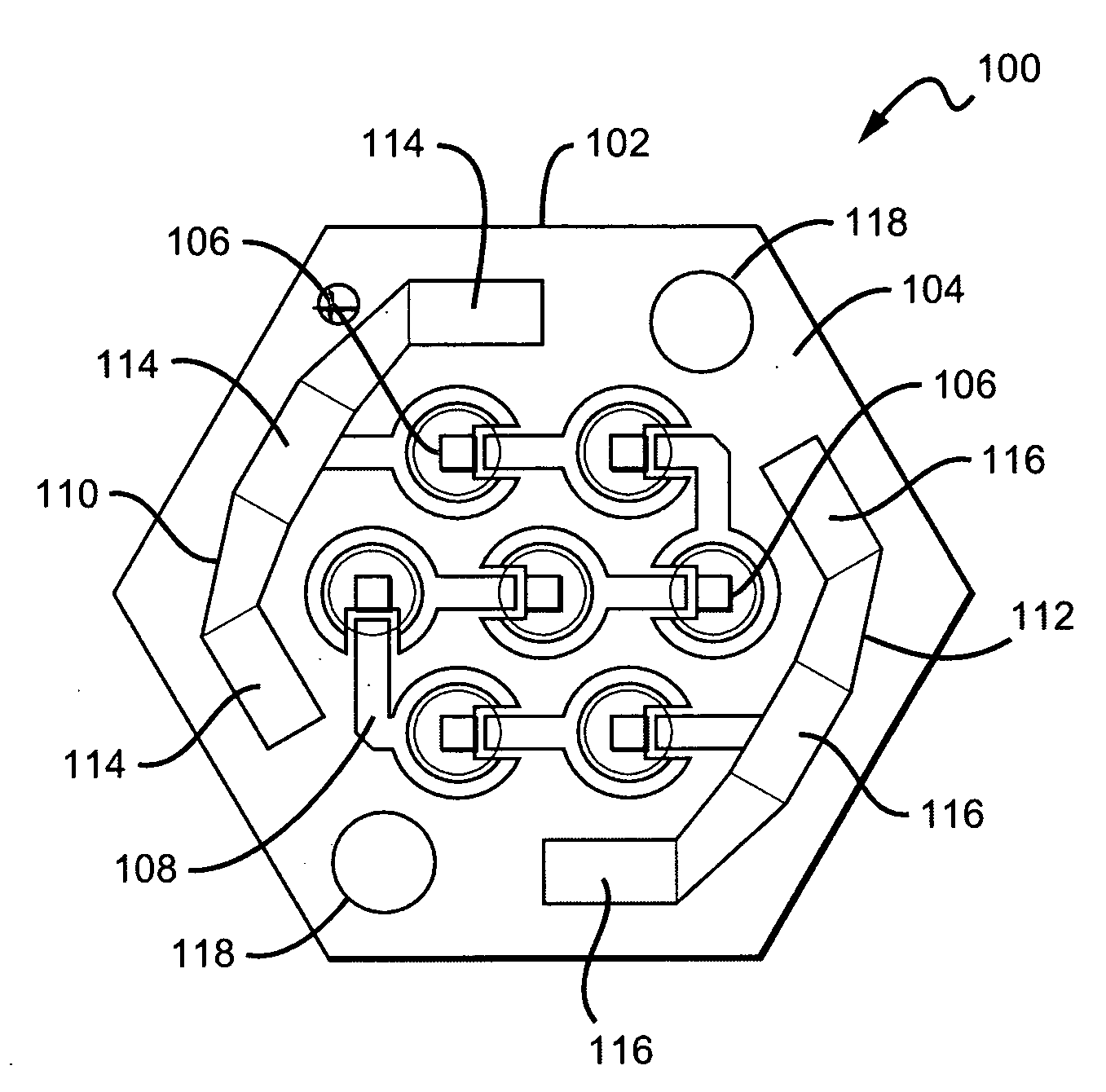
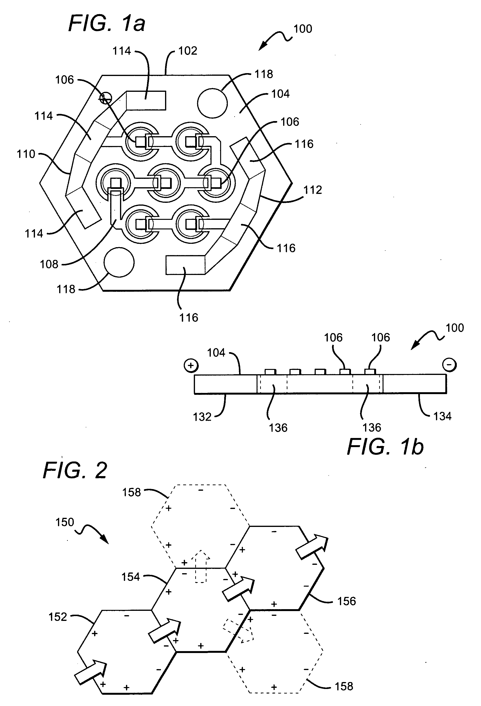
[0030]The present invention is directed to compact, simple and efficient light emitting devices or arrays and methods for manufacturing same. Each array can comprise a submount with a plurality of LEDs coupled together to emit light simultaneously when an electrical signal is applied to the array. The arrays according to the present invention can include features to provide for improved thermal management including spreading heat from the LED into the submount from where the heat can then dissipate into a heat sink attached at the bottom of device or the ambient. This allows the arrays to operate under higher power and emit higher luminous flux without overheating.

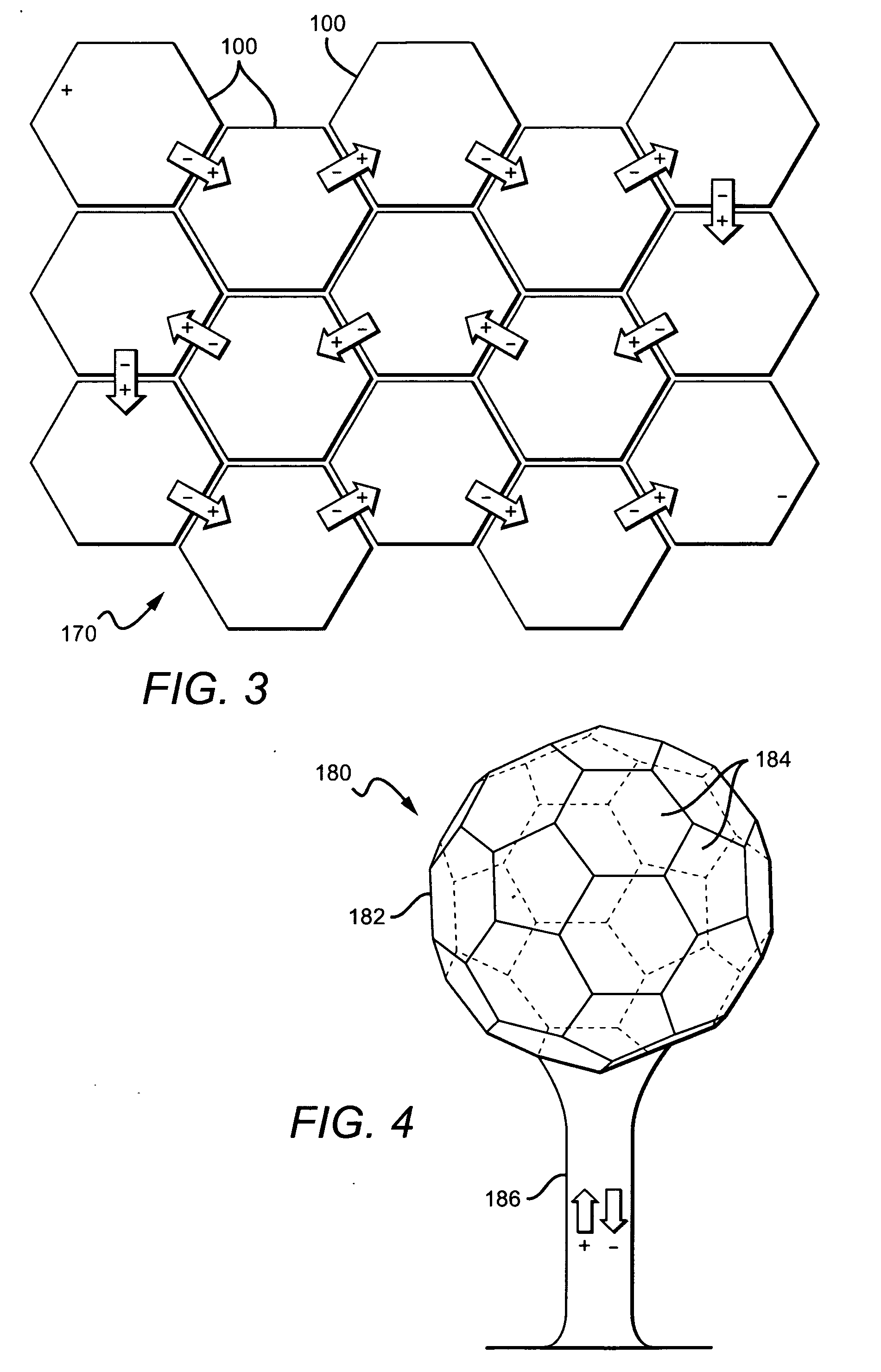
[0031]The submounts of the arrays are shaped so that multiple arrays can be mounted closely together and electrically connected to form a light source wherein all the arrays emit light in response to an electrical signal. Depending on the requirements for the particular application, different numbers of arrays can be coupl...


PUM


Abstract

A light emitting device or array comprising a submount having a top surface, a bottom surface and a plurality of edges, with input and output terminals disposed on the top surface. A plurality of attach pads and traces are also disposed on the top surface and electrically connected between the input and output terminals. A plurality of LEDs are also included, each of which is mounted to one of the attach pads. The attach pads cover more of the top surface than the LEDs and spread heat from the LEDs to the top surface of the submount. A plurality of lenses are also included each of which is molded over a respective one of the attach pads and covers the LED mounted to the particular attach pad. The arrays are shaped and arranged so that they can be easily attached to similar arrays in a tiling fashion, with the desired number of arrays included to meet the desired lighting requirements. Methods for fabricating the arrays from a single submount or submounts panel are also disclosed.

Description

[0001]This application is a continuation-in-part of and claims the benefit of U.S. patent application Ser. No. 11 / 595,720 to Yuan et al., filed on Nov. 9, 2006.[0002]The invention was made with Government support under Department of Energy Contract No. DE-FC26-05NT42340. The Government has certain rights in this invention.BACKGROUND OF THE INVENTION[0003]1. Field of the Invention[0004]The invention relates to lighting systems, and more particularly to interconnected light emitting diode (LED) arrays.[0005]2. Description of the Related Art[0006]LEDs are semiconductor photon sources that can serve as highly efficient electronic-to-photonic transducers. They are typically forward-biased p-n junctions fabricated from a semiconductor material that emits light via injection electroluminescence. Their small size, high efficiency, high reliability, and compatibility with electronic systems make them very useful for a multitude of applications. Recent advancements have yielded high-power LED...

Claims


Application Information

Patent Timeline
IPC IPC(8): F21V5/00H01L33/00H01L21/60H01L33/62
CPCF21K9/00F21S2/005F21V5/007F21Y2113/00H01L25/0753H01L33/62F21Y2105/10H01L2924/0002F21Y2115/10F21Y2107/40F21V5/04H01L2924/00F21V5/10
Inventor YUAN, THOMAS CHENG-HSINKELLER, BERND
Owner CREELED INC
Why Eureka
Try Eureka