Semiconductor storage device
- Summary
- Abstract
- Description
- Claims
- Application Information
AI Technical Summary
Benefits of technology
Problems solved by technology
Method used
Image

Examples
first embodiment
[0039]A first embodiment of the present invention will now be described below.
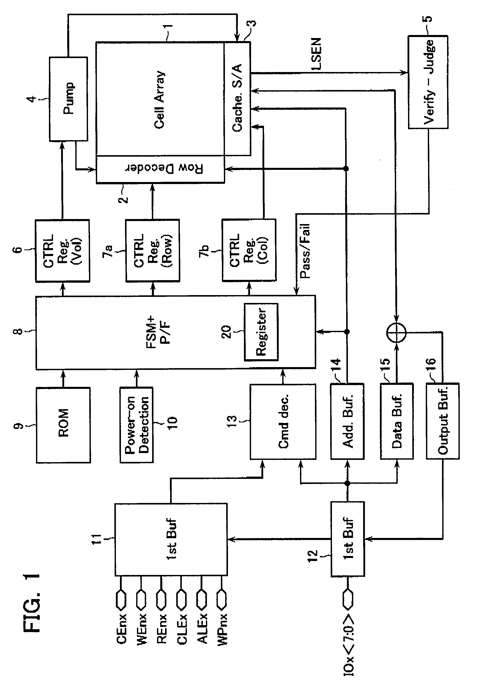
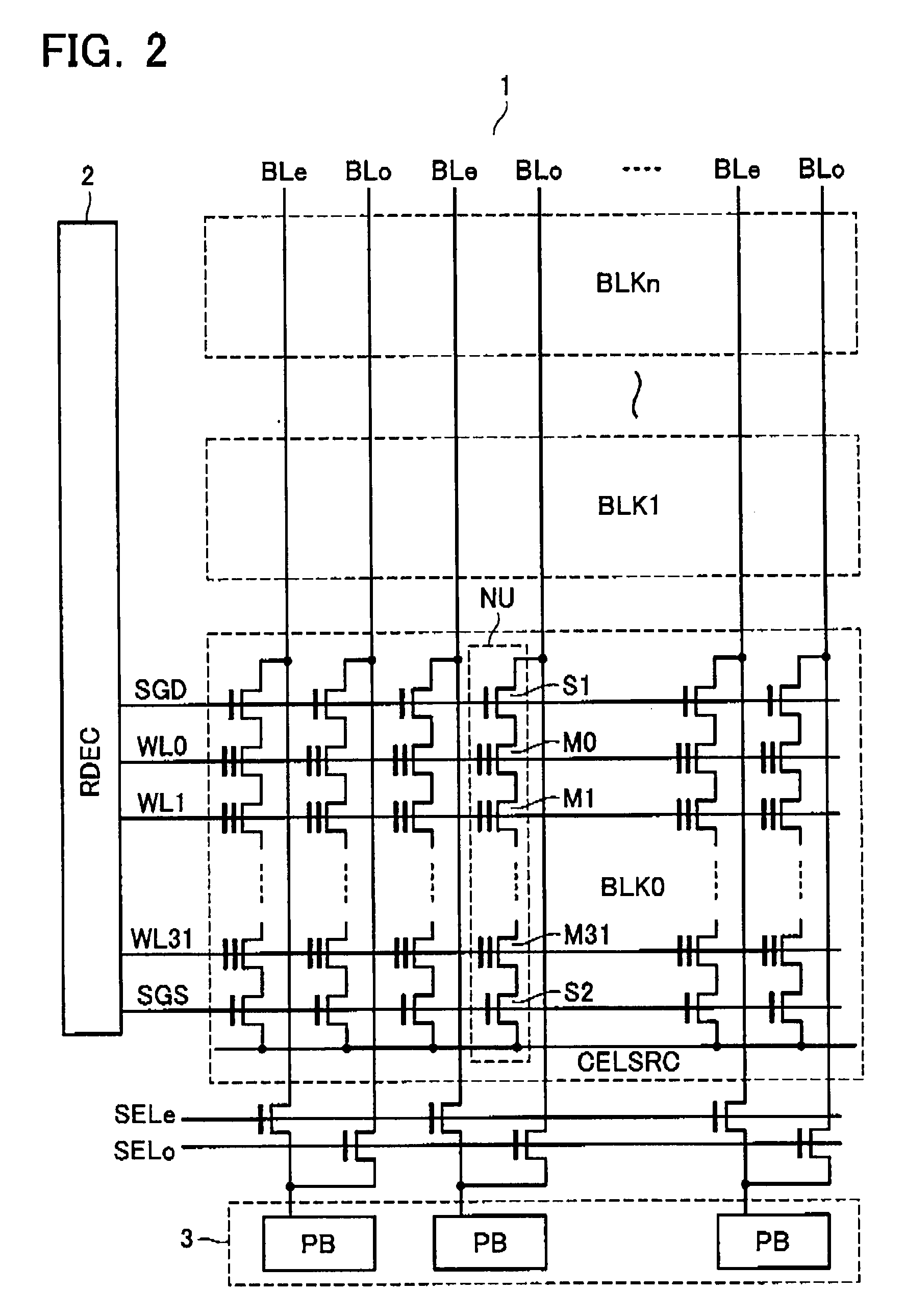
[0040]FIG. 1 illustrates a functional block configuration for a NAND-type flash memory according to this embodiment; and FIG. 2 illustrates a cell array configuration of the memory core part in the NAND-type flash memory. As illustrated in FIG. 2, a cell array 1 comprises a series of NAND cell units (NAND strings) NU, each having a plurality of electrically rewritable non-volatile memory cells (in this example, 32 memory cells MC) M0-M31 connected in series.
[0041]One end of each of the NAND cell units NU is connected to a respective bit line BLo (odd-numbered) and BLe (even-numbered) via a respective selection gate transistor S1, and the other end connected to a common source line CELSRC via a respective selection gate transistor S2. A control gate of each of the memory cells M0-M31 is connected to a respective word line WL0-WL31. The gate of each of the selection gate transistors S1 and S2 is connected to...
second embodiment
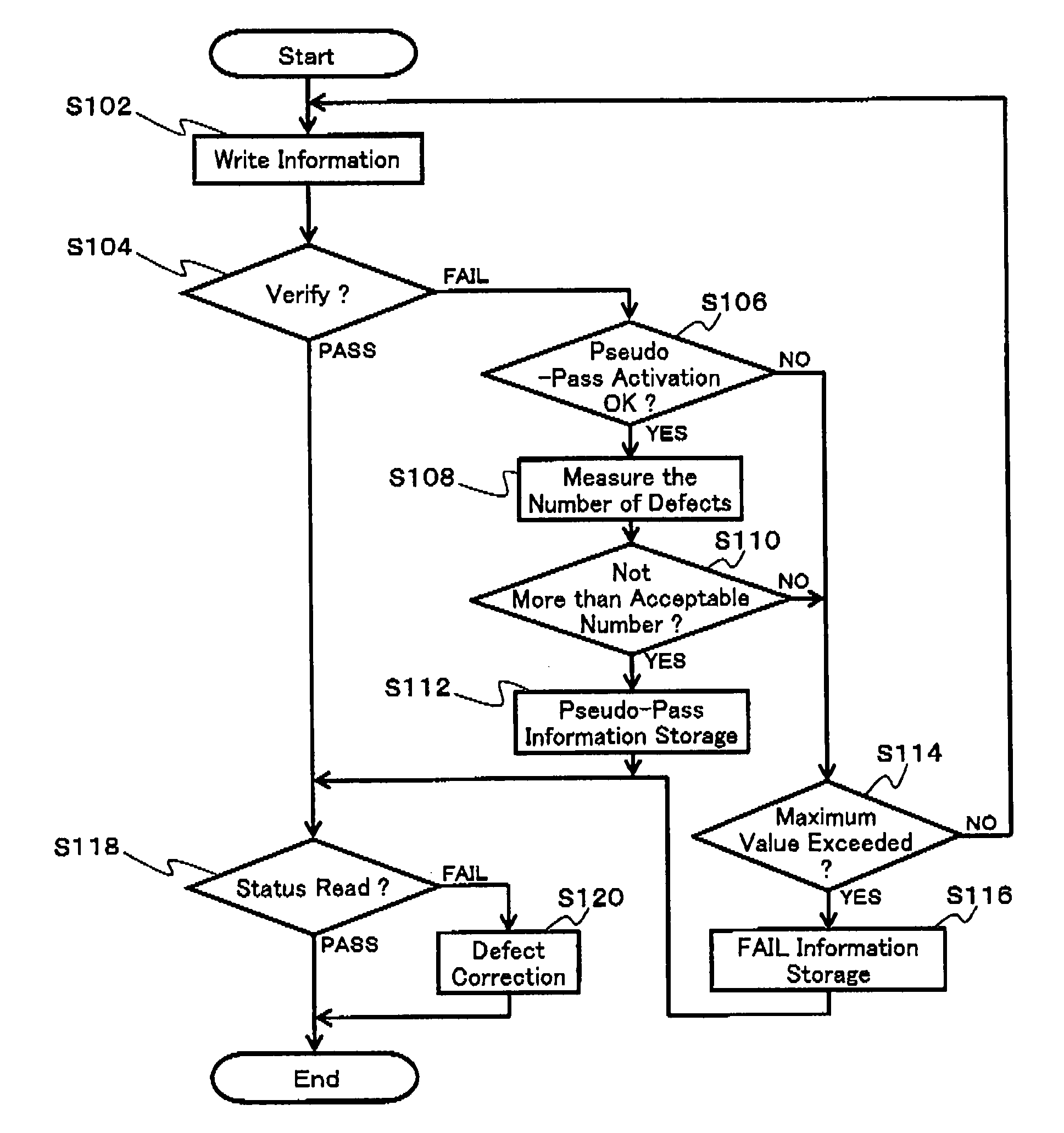
[0124]A write verify operation according to a second embodiment will now be described below. The NAND-type flash memory of the semiconductor storage device according to this embodiment is, similar to the first embodiment, a multi-value storage memory that may store 2 bits in one memory cell. This embodiment includes a verify operation that involves a step of performing a verify skip operation. Specifically, at the beginning of the write operation to a memory cell, the amount of threshold voltage shift is small and so is the number of memory cells that reach their verify levels. Thus, performing a verify read at this stage would result in “FAIL”. In addition, performing a pseudo-pass-judge at this state would likely result in “FAIL”. Thus, what would reduce the total amount of time for writing is not performing any verify read at this stage. Therefore, conditions for a predetermined verify skip are defined and a determination is made as to whether the verify operation is to be skippe...
third embodiment
[0178]A third embodiment will now be described below. The third embodiment has a pseudo-pass setting fixed to zero for the data “2” in the corresponding memory cell of the second page of the first or second embodiment. Thus, only the complete PASS is permitted for the data “2” in the corresponding memory cell of the second page. The NAND-type flash memory according to this embodiment has the smaller amount of threshold-voltage shift in writing, for the data “2” in the corresponding memory cell of the second page, in comparison to each of data “2*” in the corresponding memory cell of the first page, data “1” in the corresponding memory cell of the second page, and data “3” in the corresponding memory cell. Therefore, it is likely that the complete PASS would be provided, and thus the number of pseudo-pass setting is set to “0” for the data “2” in the corresponding memory cell of the second page. This allows registers to be omitted that is used to store pseudo-pass information for the...
PUM
 Abstract
Description
Claims
Application Information
 - R&D Engineer
- R&D Manager
- IP Professional
- Industry Leading Data Capabilities
- Powerful AI technology
- Patent DNA Extraction
Browse by: Latest US Patents, China's latest patents, Technical Efficacy Thesaurus, Application Domain, Technology Topic.
© 2024 PatSnap. All rights reserved.Legal|Privacy policy|Modern Slavery Act Transparency Statement|Sitemap