Stress free package and laminate-based isolator package

a stress-free, isolator technology, applied in the direction of semiconductor devices, semiconductor/solid-state device details, electrical apparatus, etc., can solve the problems of temperature coefficient mismatch, fluctuation in product performance and reliability, negative impact of the die of the simonductor, etc., to reduce stress, reduce stress, reduce stress

Inactive Publication Date: 2008-07-24
ANALOG DEVICES INC
View PDF8 Cites 40 Cited by
  • Summary
  • Abstract
  • Description
  • Claims
  • Application Information

AI Technical Summary

Benefits of technology

[0023]The present invention also provides for a method to reduce stress in a semiconductor package comprising: (a) depositing an anisotropic conducting film (ACF) on a semiconductor die, said ACF film further containing gold stud bumps; and (b) forming an air gap by contacting the semiconductor die having the deposited ACF film with gold stud bumps with a lead frame, wherein the formed air gap prevents underfill or molding compound from coming in contact with said stress sensitive area on the semiconductor die.
[0024]The present invention also provides for a method to reduce stress in a semiconductor package comprising: (a) depositing a continuous anisotropic conducting film (ACF) on a semiconductor die, said ACF film further having a plurality of gold stud bumps dispersed within; an

Problems solved by technology

A semiconductor die can be negatively impacted by the packaging process.
This direct contact can cause a fluctuation in the performance and reliability of the product.
In high-performance semiconductor packaging structures, a temperature coefficient mismatch occurs due to t

Method used


Image

  • Stress free package and laminate-based isolator package
  • Stress free package and laminate-based isolator package
  • Stress free package and laminate-based isolator package

Examples


Embodiment Construction

[0046]While this invention is illustrated and described in a preferred embodiment, the invention may be produced in many different configurations. There is depicted in the drawings, and will herein be described in detail, a preferred embodiment of the invention, with the understanding that the present disclosure is to be considered as an exemplification of the principles of the invention and the associated functional specifications for its construction and is not intended to limit the invention to the embodiment illustrated. Those skilled in the art will envision many other possible variations within the scope of the present invention.

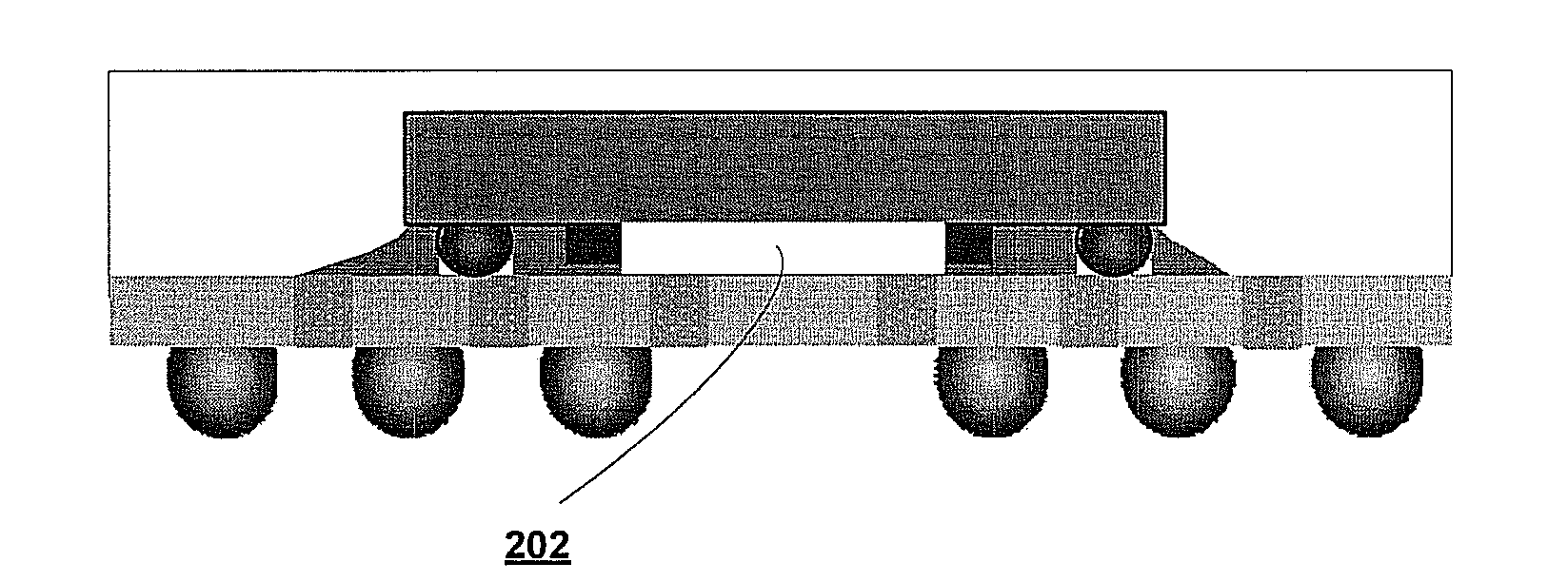
[0047]FIG. 1 illustrates a stress free region packaging according to one aspect of the present invention wherein an air cavity is created by depositing a perimeter 102, preferably made of polymer, around an element in the semiconductor die that is susceptible to stress. Although the specific example of polymer is used, it should be noted that other mat...


PUM


Abstract

Various methods are described where the semiconductor die and the lead frame (or the BGA or LGA substrate) are spaced apart to reduce stress. In one scenario, an air gap is formed between the semiconductor die and the lead frame by depositing a perimeter (made, for example, using polymer) either on the semiconductor die or the lead frame. In another scenario, an anisotropic conducting film (ACF) is formed with an air gap between the semiconductor die and the lead frame (or the BGA or LGA substrate). The air gap relieves stress on the semiconductor die. Further, a lead frame-based isolator package and a BGA (or LGA) isolator package are described. A window-frame ACF-based isolation method for magnetic coupling in a lead-frame package and BGA (or LGA) package is also described.

Description

BACKGROUND OF THE INVENTION[0001]1. Field of Invention[0002]The present invention relates generally to the field of semiconductor packaging. More specifically, the present invention is related to a stress free package having a stress free region and a laminate-based isolator package.[0003]2. Discussion of Prior Art[0004]A semiconductor die can be negatively impacted by the packaging process. The packaging process typically entails encapsulating the semiconductor device with a plastic mold compound or other polymer based encapsulant. This process results in direct physical contact between the semiconductor die surface with its active components and the mold compound encapsulant. This direct contact can cause a fluctuation in the performance and reliability of the product. In high-performance semiconductor packaging structures, a temperature coefficient mismatch occurs due to the uneven expansion of the mold as compared to the silicon die whereby localized stress caused by the expansi...

Claims


Application Information

Patent Timeline
IPC IPC(8): H01L21/00
CPCH01L21/563H01L2224/14051H01L23/49816H01L24/12H01L24/32H01L24/83H01L2224/13099H01L2224/16225H01L2224/27013H01L2224/48091H01L2224/48247H01L2224/49171H01L2224/49175H01L2224/73203H01L2224/83051H01L2224/838H01L2924/01005H01L2924/01013H01L2924/01057H01L2924/01079H01L2924/01082H01L2924/0781H01L2924/12044H01L2924/15311H01L2924/19043H01L2924/3511H01L23/315H01L2224/26175H01L2924/10253H01L2224/73204H01L2224/32225H01L2224/16245H01L2924/0665H01L2924/014H01L2924/01076H01L2924/01006H01L2224/2919H01L24/49H01L24/48H01L2924/00014H01L2924/00H01L2924/181H01L2224/05554H01L2224/4826H01L2924/18165H01L2224/45144H01L24/45H01L2924/00011H01L2224/0401H01L2924/00012H01L2224/45015H01L2924/207
Inventor SENGUPTA, DIPAKGOIDA, THOMAS
Owner ANALOG DEVICES INC
Why Eureka
Try Eureka