Semiconductor device and method of fabricating the same

a technology of semiconductor devices and semiconductors, applied in the direction of semiconductor/solid-state device details, pulse techniques, logic circuits, etc., can solve the problem of not allowing a large number of capacitive elements to be disposed on an lsi having a relatively high integrated density, and achieve the effect of efficient suppression of power noise of an lsi

Inactive Publication Date: 2008-07-31
NEC ELECTRONICS CORP
View PDF1 Cites 124 Cited by
  • Summary
  • Abstract
  • Description
  • Claims
  • Application Information

AI Technical Summary

Benefits of technology

[0010]According to the technique of the present invention, it is possible to efficiently suppress the power noise of an LSI, particularly, an LSI having the multi-level mesh source interconnection structure.

Problems solved by technology

A variety of attempts have been made for reduction in noise of LSIs, which is an important challenge.
This approach, however, has to provide an area required for the capacitive elements to be disposed and hence cannot allow a large number of capacitive elements to be disposed on an LSI having a relatively high integrated density.

Method used


Image

  • Semiconductor device and method of fabricating the same
  • Semiconductor device and method of fabricating the same
  • Semiconductor device and method of fabricating the same

Examples


first embodiment

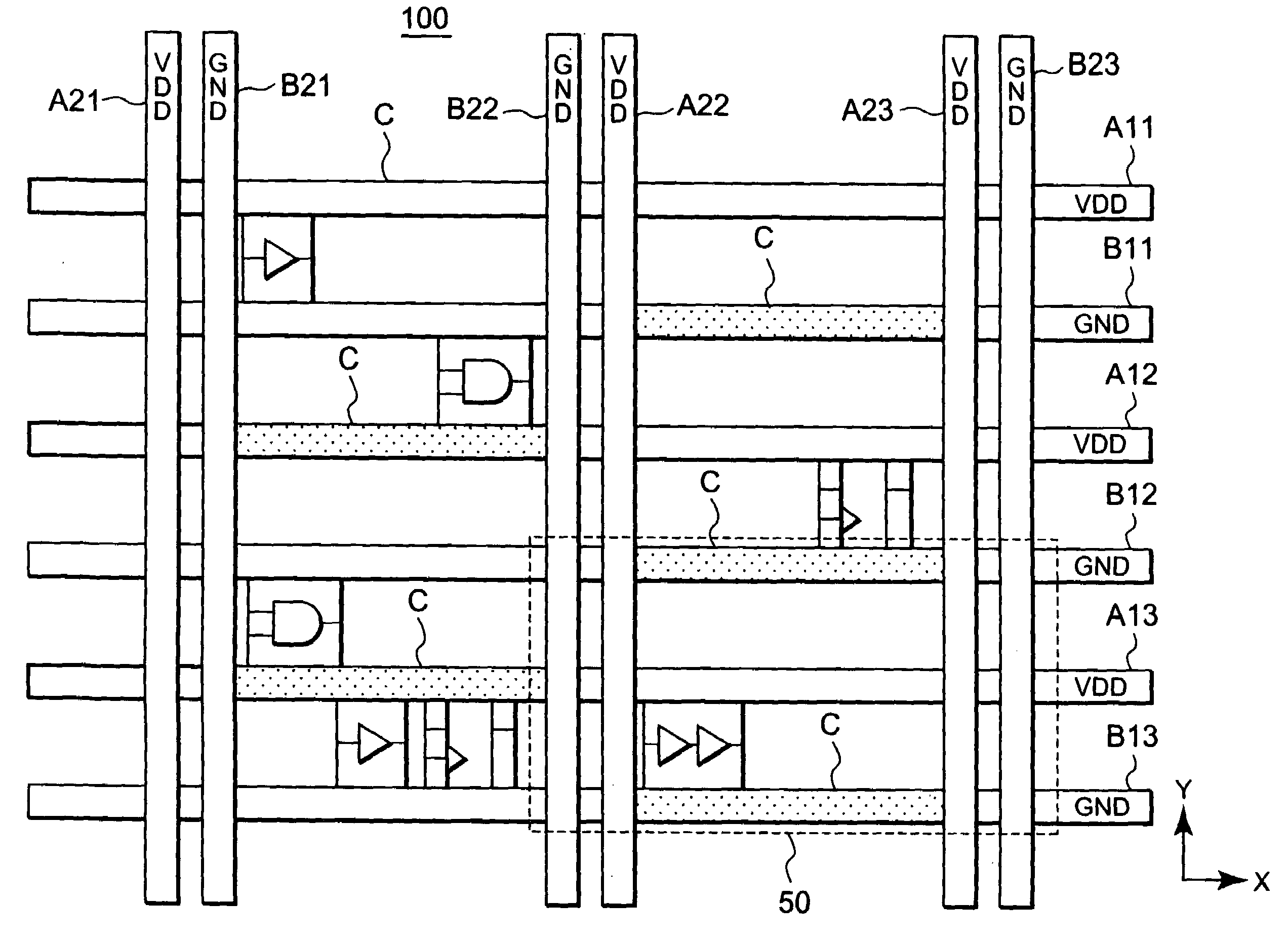
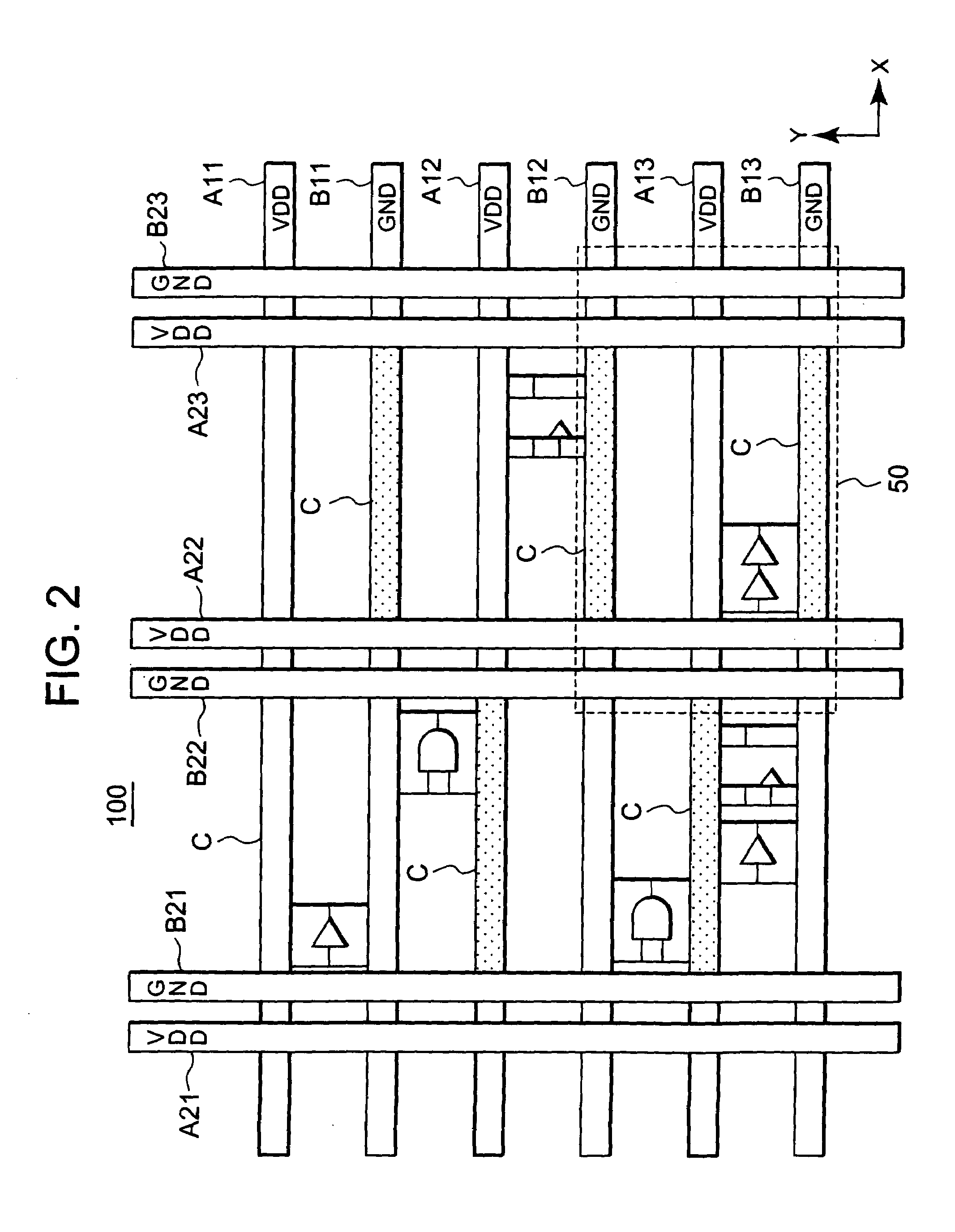
[0022]FIG. 2 is a plan view, as viewed from above, showing a semiconductor device 100 according to a first embodiment of the present invention. The semiconductor device 100, together with hard macro cells such as a memory device and a CPU core, forms an LSI chip. As shown, the semiconductor device 100 has logic elements, and VDD lines and GND lines for supplying a source voltage and a reference voltage (i.e., ground voltage in the example illustrated here), respectively, to these logic elements.

[0023]In the semiconductor device 100, interconnection for supplying power to the logic elements has a two-level mesh structure. VDD lines All, A12, and A13 and GND lines B11, B12, and B13 shown are arranged alternately in an interconnection layer lying above the logic elements (hereinafter will be referred to as “first interconnection layer”). These supply lines are positioned to extend in the same direction as the X-direction in which the logic elements are arranged.

[0024]Above the first in...

second embodiment

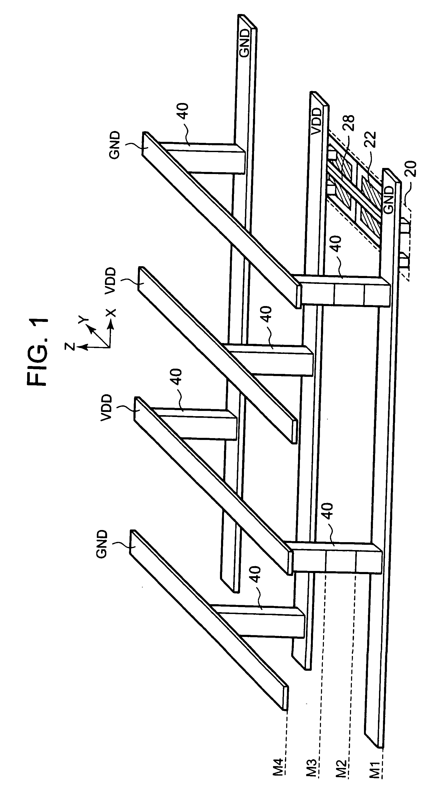
[0039]FIG. 4 shows a cutout portion 60, corresponding to the cutout portion 50 shown in FIG. 3, of a semiconductor device according to a second embodiment of the present invention. Like reference characters are used designate like or corresponding parts throughout FIGS. 3 and 4 in order to omit detailed description thereof.

[0040]While the foregoing semiconductor device 100 according to the first embodiment has the four metal layers M1 to M4, a semiconductor device according to the present invention can be realized without the provision of the metal layers M2 and M3, i.e., with the provision of only two metal layers M1 and M4. Though the second embodiment shown in FIG. 4 has two metal layers, the reference characters M1 and M4 each remain the same to designate the two metal layers for simplification of description.

[0041]In the case of the provision of only two metal layers as shown in FIG. 4, VDD lines D31 and D32 are positioned in the second metal layer M4 and connected directly to ...


PUM


Abstract

This invention efficiently suppresses the power noise of an LSI. A semiconductor device includes first and second interconnection layers. The first interconnection layer has a source voltage supply line of a first potential positioned to extend along logic cells in a first direction. The second interconnection layer lies on an upper layer than the first interconnection layer and has plural source voltage supply lines of a second potential arranged adjacent to each other to form a group and positioned to extend in a second direction which is different from the first direction of interconnection. An interconnection line of the second potential is positioned on an upper layer than the first interconnection layer and interconnects at least two of the plurality of source voltage supply lines of the second potential. The interconnection line of the second potential is positioned to overlap the source voltage supply line of the first potential, to form a capacitor with the source voltage supply line of the first potential.

Description

BACKGROUND OF THE INVENTION[0001]1. Field of the Invention[0002]The present invention relates to semiconductor devices and more particularly to a semiconductor device having source interconnection of a multi-level mesh structure, and a method of fabricating the same.[0003]2. Description of Related Art[0004]In recent years, the integrated density of semiconductor LSIs (integrated circuits) has been raised increasingly. The multi-level mesh source interconnection technique for power supply has been frequently employed in LSIs in order to reduce the area occupied by the interconnection for power supply and make the interconnection designing flexible. Specifically, the multi-level mesh source interconnection technique is such that: plural source interconnection layers are formed vertically over logic elements; in each of the source interconnection layers a source voltage supply line (hereinafter will be referred to as “VDD line”) and a reference voltage supply line (e.g., ground voltage...

Claims


Application Information

Patent Timeline
Patent Type & Authority Applications(United States)
IPC IPC(8): H03K19/00
CPCH01L23/5223H01L23/5286H01L27/0207H01L27/11898H01L2924/0002H01L2924/00
Inventor ISHIKAWA, HIROTAKA
Owner NEC ELECTRONICS CORP
Why Eureka
Try Eureka