Semiconductor package

a technology of semiconductors and components, applied in the direction of semiconductor devices, semiconductor/solid-state device details, electrical apparatus, etc., can solve the problems of increasing the number of external connection pins of leadframe packages, increasing the cost of packaging accordingly, and increasing the complexity of integrated circuit chips

Active Publication Date: 2016-08-02
MEDIATEK INC
View PDF15 Cites 0 Cited by
  • Summary
  • Abstract
  • Description
  • Claims
  • Application Information

AI Technical Summary

Benefits of technology

[0008]In light of the above, there is a strong need in this industry to provide an improved semiconductor package structure and leadframe package, which are cost-effective, particularly suited for high-speed semiconductor dies, and are capable of improving power supply variations and suppressing power noise.

Problems solved by technology

The integrated circuit chip is becoming more and more complicated, leading to increased number of external connection pins of the leadframe package.
As the pin count is increased, the cost of packaging is increased accordingly.
Further, as the integration and performance of semiconductor dies increase, the impact of power noise on I / O signaling is significant.
The crowded wires bonded to one single lead result in reliability and yield issues.

Method used


Image

  • Semiconductor package
  • Semiconductor package
  • Semiconductor package

Examples


Embodiment Construction

[0020]The present invention pertains to an improved semiconductor package, as described below, which is suited for the applications including, but not limited to, LQFP (Low-Profile Quad Flat Pack) packaging, TQFP (Thin Quad Flat Pack) packaging, QFN (Quad Flat Non-leaded) packaging, DFN (Dual Flat No-lead) packaging, multi-zone QFN, multi-die flip-chip packaging, and other applicable packaging technology.

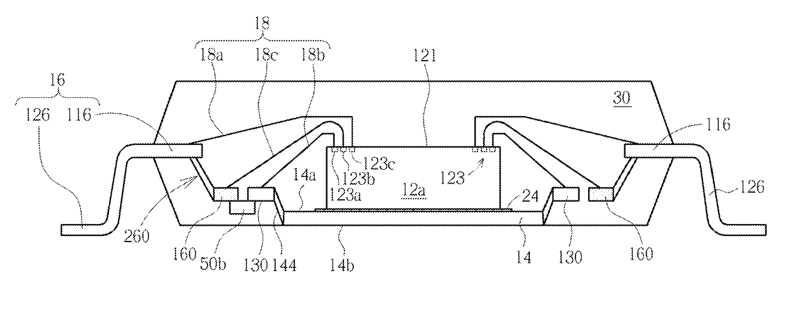
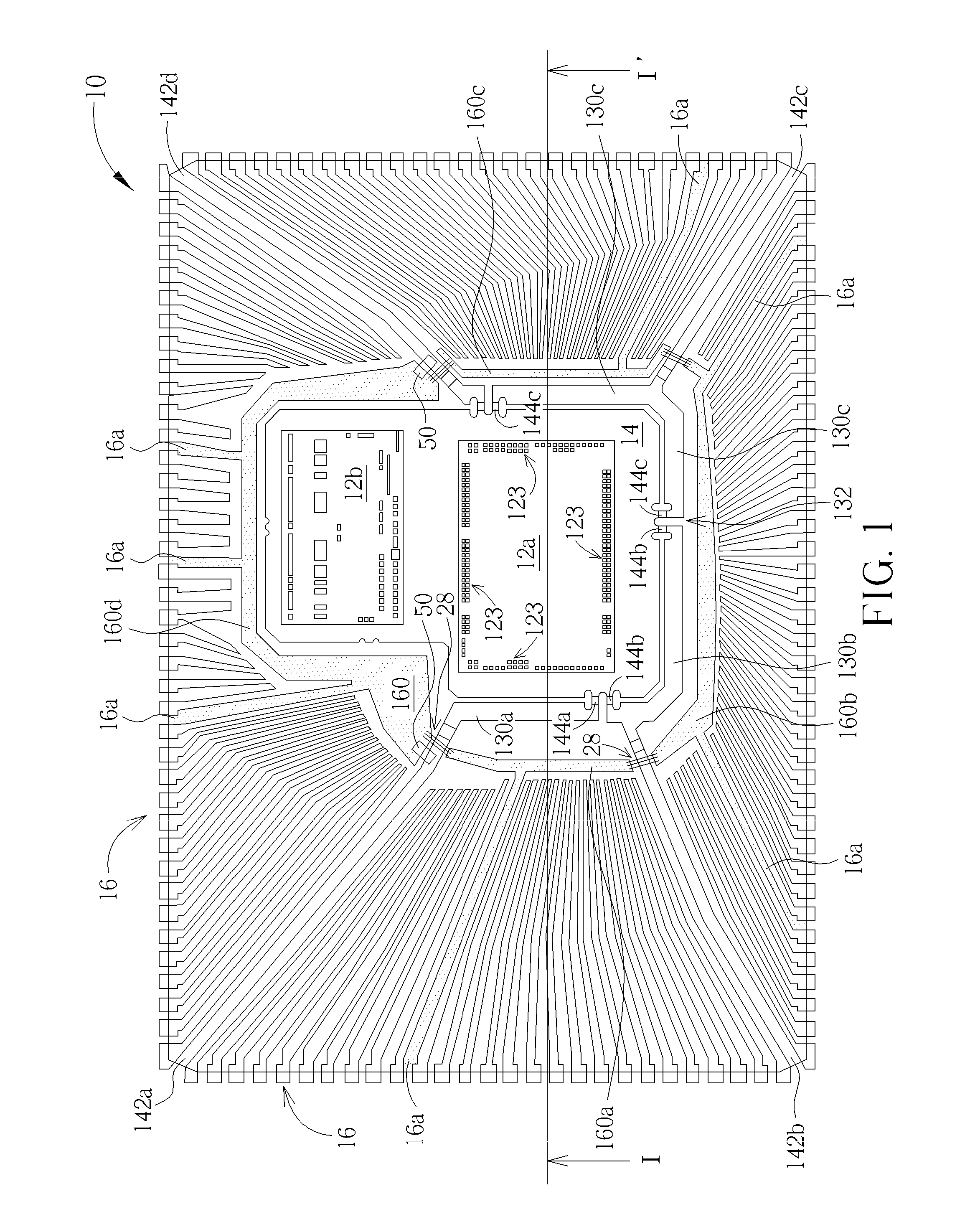
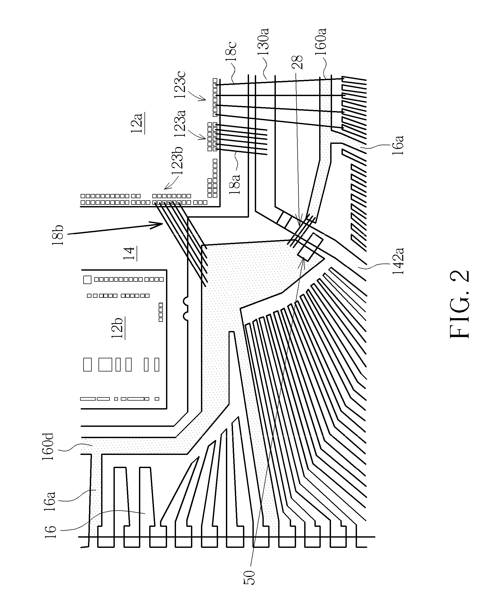
[0021]Please refer to FIGS. 1-3. FIG. 1 illustrates a schematic top view of an exemplary leadframe package 10 according to one embodiment of the invention. FIG. 2 is an enlarged top view showing a germane portion of the leadframe package 10. FIG. 3 is a schematic, cross-sectional view taken along line I-I′ of FIG. 1. As shown in FIGS. 1-3, in general, the leadframe package 10 includes at least one semiconductor die 12a that is mounted on a die pad 14 and is adhered to a top surface 14a of the die pad 14 by using an adhesive 24 such as silver paste or epoxy. According to one embodime...


PUM


Abstract

A semiconductor package includes a die pad, wherein a semiconductor die is mounted on the die pad; a plurality of leads comprising a power lead disposed along a peripheral edge of the die pad; at least one connecting bar connecting with the die pad; and a power bar disposed on one side of the connecting bar, wherein the power bar is integrally connected to the power lead. A capacitor is mounted between the power bar and the connecting bar.

Description

CROSS REFERENCE TO RELATED APPLICATIONS[0001]This is a continuation of U.S. application Ser. No. 13 / 626,899 filed Sep. 26, 2012, which claims the benefit of U.S. provisional application No. 61 / 541,235, filed Sep. 30, 2011.BACKGROUND OF THE INVENTION[0002]1. Field of the Invention[0003]The present invention relates generally to integrated circuit (IC) package technology. More particularly, the present invention relates to a semiconductor package including a leadframe with power bars or power ring, which is capable of improving power supply variations and suppressing power noise.[0004]2. Description of the Prior Art[0005]Semiconductor dies are conventionally enclosed in plastic packages that provide protection from harsh environments and enable electrical interconnection between the semiconductor die and a substrate or circuit board. Such an integrated circuit (IC) package typically includes a metal substrate or a leadframe, a semiconductor die mounted on a die pad of the leadframe, a...

Claims


Application Information

Patent Timeline
Patent Type & Authority Patents(United States)
IPC IPC(8): H01L23/48H01L23/495
CPCH01L23/49541H01L23/49575H01L23/49589H01L23/49503H01L2224/73265H01L2224/32245H01L2224/49109H01L2924/00H01L2224/48257H01L2224/48247H01L2224/49113H01L2224/49171H01L2924/3011H01L23/49517H01L2924/181H01L2224/48095H01L2924/00012H01L24/49H01L2224/49175H01L2224/29294H01L24/29H01L24/48H01L2224/29339H01L2924/19107H01L2224/04042H01L2924/19043H01L24/32H01L2224/49177H01L2924/19105H01L2224/2919H01L2224/48091H01L2224/05554H01L2924/19041H01L2924/00014H01L2224/45099
Inventor CHEN, NAN-JANG
Owner MEDIATEK INC
Why Eureka
Try Eureka