Semiconductor integrated circuit device and manufacturing method thereof
一种集成电路、制造方法的技术,应用在半导体/固态器件制造、半导体器件、电路等方向,能够解决寄生电阻63增大、集成电路动作速度降低、去耦效果降低等问题,达到削减电源噪声、防止动作速度的降低、抑制电源噪声的效果
- Summary
- Abstract
- Description
- Claims
- Application Information
AI Technical Summary
Problems solved by technology
Method used
Image

Examples
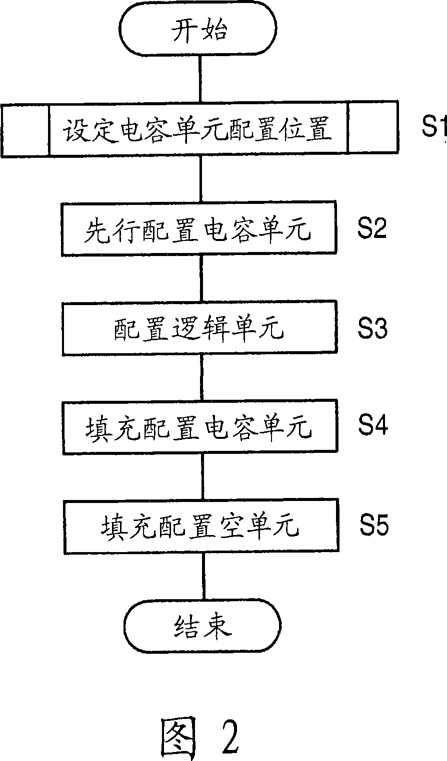
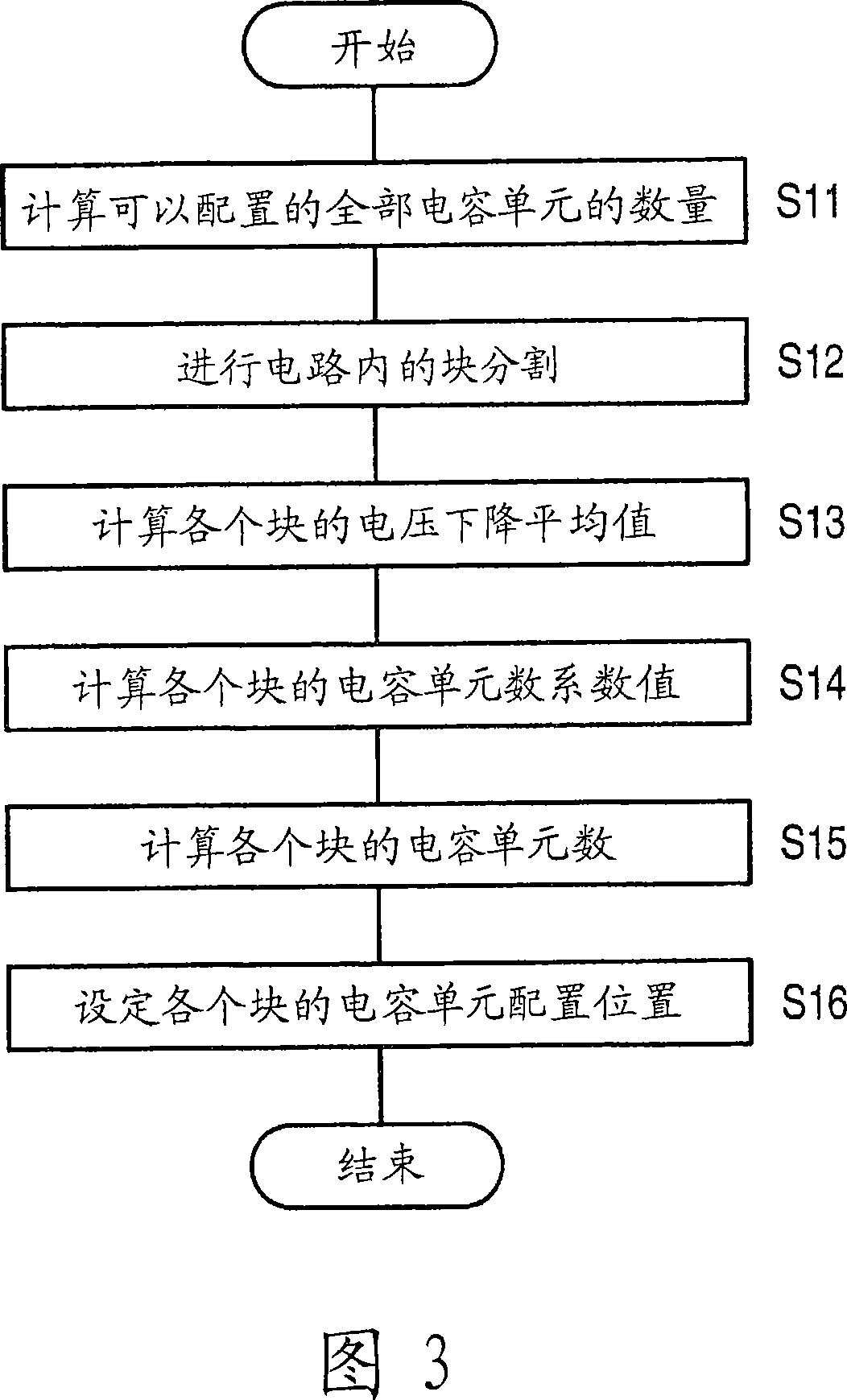
Embodiment
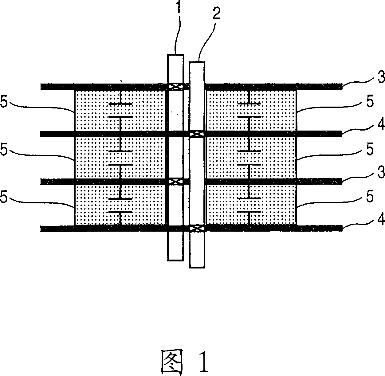
[0028] FIG. 1 is an explanatory diagram of a semiconductor integrated circuit device in which a capacitor unit is arranged according to an embodiment.
[0029] In FIG. 1 , 1 indicates the main power line, 2 indicates the main grounding line, 3 indicates the main power line, and 4 indicates the main grounding line.
[0030] 5 denotes a capacitor unit, which is arranged near the main power supply line 1 and the main ground line 2 . The capacitor unit 5 is a capacitor unit whose capacitance per unit area is greater than 1, and the capacitor unit 5 is arranged near the main power line 1 and the main ground line 2 . Also, although not shown, the logic cells constituting the semiconductor integrated circuit are arranged in an area other than the area in which the capacitor cells 5 are arranged after the capacitor cells 5 are preferentially arranged.
[0031] Among them, one logic cell corresponds to an area where one inverter element (composed of one PMOS and one MMOS) is formed. ...
PUM
 Abstract
Description
Claims
Application Information
 - R&D
- Intellectual Property
- Life Sciences
- Materials
- Tech Scout
- Unparalleled Data Quality
- Higher Quality Content
- 60% Fewer Hallucinations
Browse by: Latest US Patents, China's latest patents, Technical Efficacy Thesaurus, Application Domain, Technology Topic, Popular Technical Reports.
© 2025 PatSnap. All rights reserved.Legal|Privacy policy|Modern Slavery Act Transparency Statement|Sitemap|About US| Contact US: help@patsnap.com