Boosting charge pump circuit
a charge pump and circuit technology, applied in the direction of power conversion systems, instruments, dc-dc conversion, etc., can solve the problem avoid providing charge pump capacitance, avoid having an unused area on a semiconductor chip, and avoid the effect of wasting chip area
- Summary
- Abstract
- Description
- Claims
- Application Information
AI Technical Summary
Benefits of technology
Problems solved by technology
Method used
Image
Examples
first embodiment
[0055](Boosting Charge Pump Circuit Applied to DDR1 Specifications)
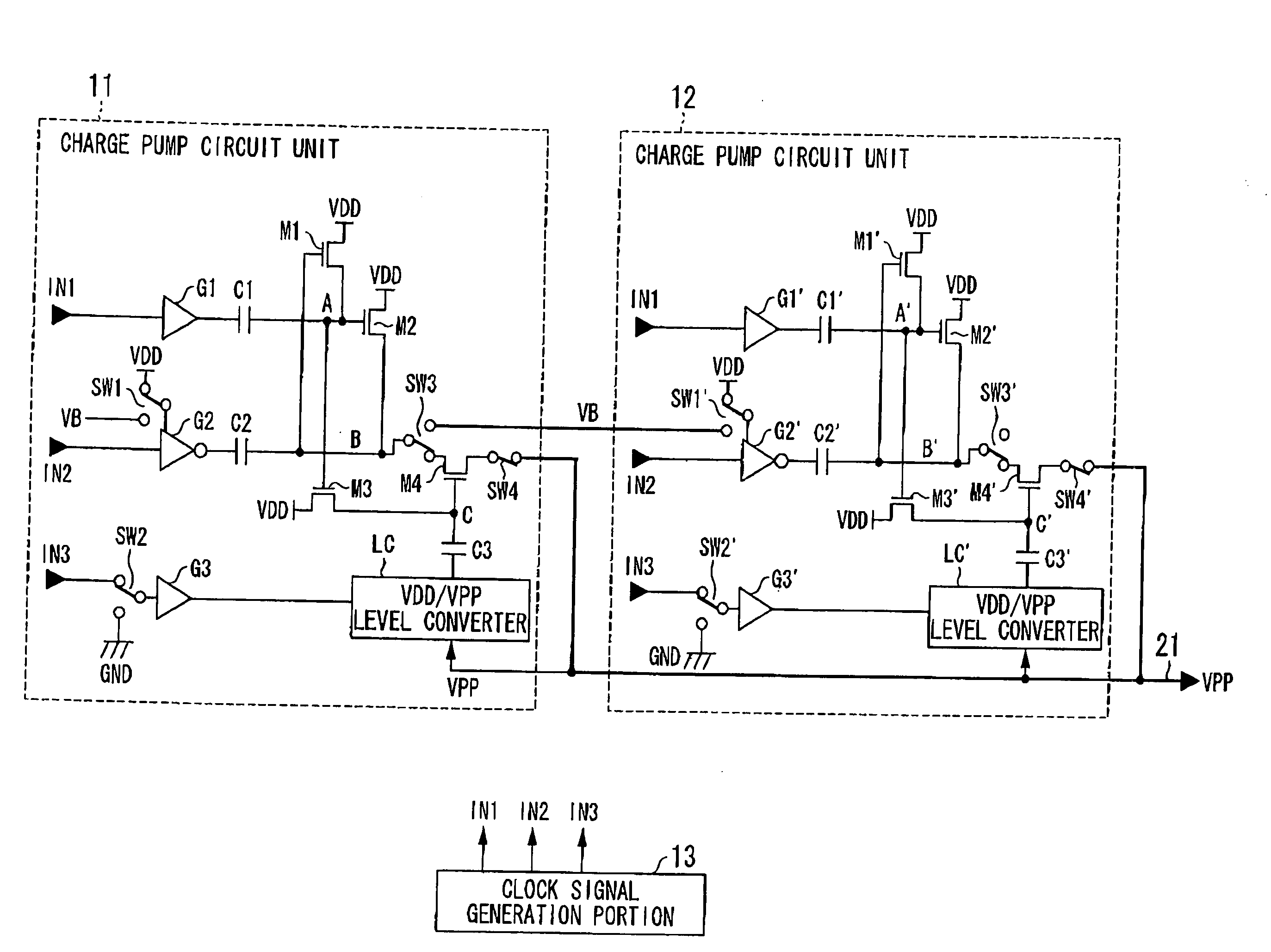
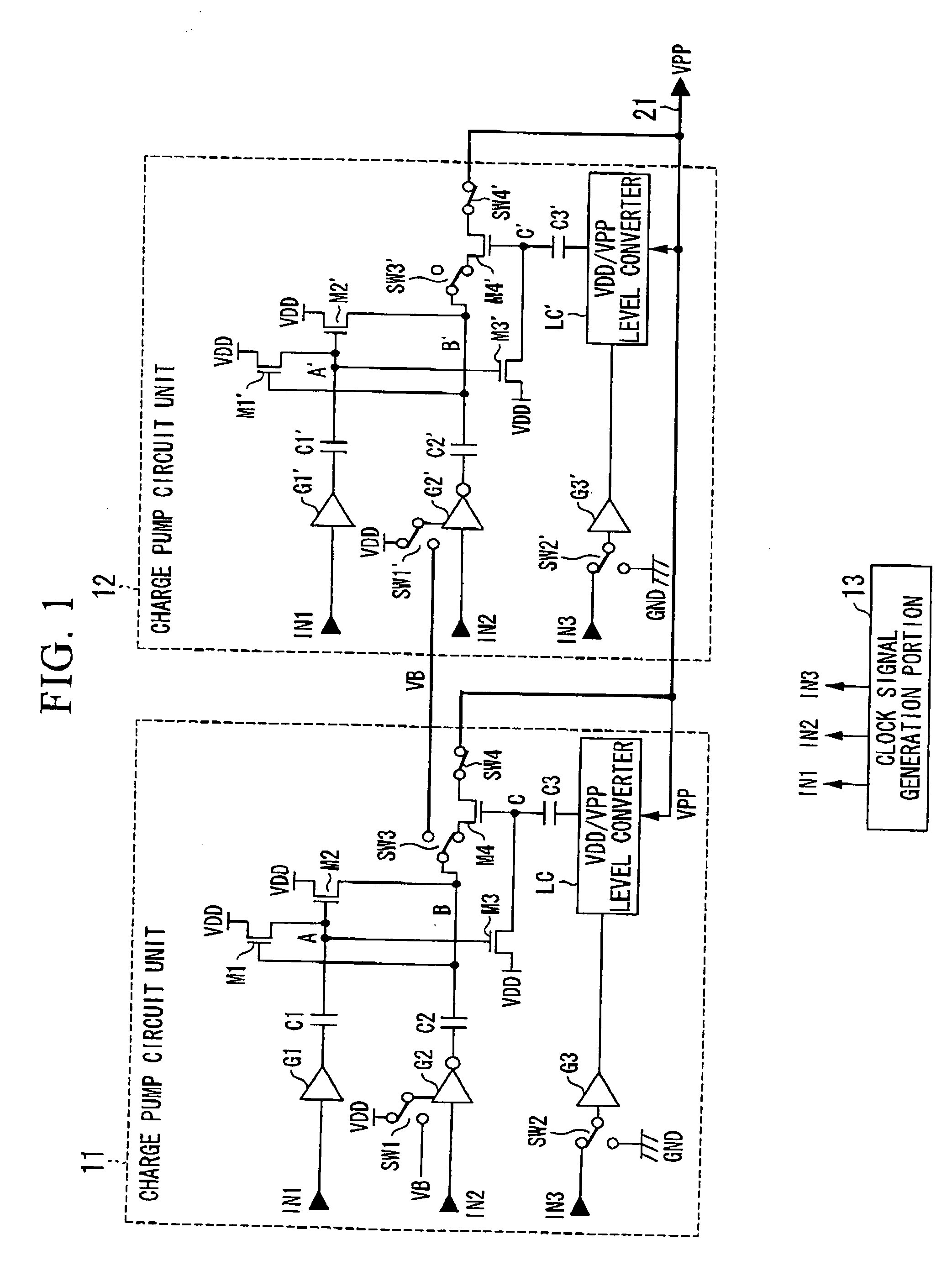
[0056]FIG. 1 is a drawing which shows a constitution of a boosting charge pump circuit of a first embodiment. FIG. 1 shows an example of a boosting charge pump circuit which is applied with DDR1 specifications (for example, a power supply voltage is 2.5V).
[0057]The boosting charge pump circuit shown in FIG. 1 is constituted from two charge pump circuit units 11 and 12. Both the charge pump circuit units 11 and 12 have the same constitution. The power supply voltage (external power supply voltage) VDD is boosted by operating both the charge pump circuit units 11 and 12 in parallel so as to adjust the internal voltage (internal power supply voltage) VPP of the internal power line 21 in a range of “2×VDD>VPP>VDD”.
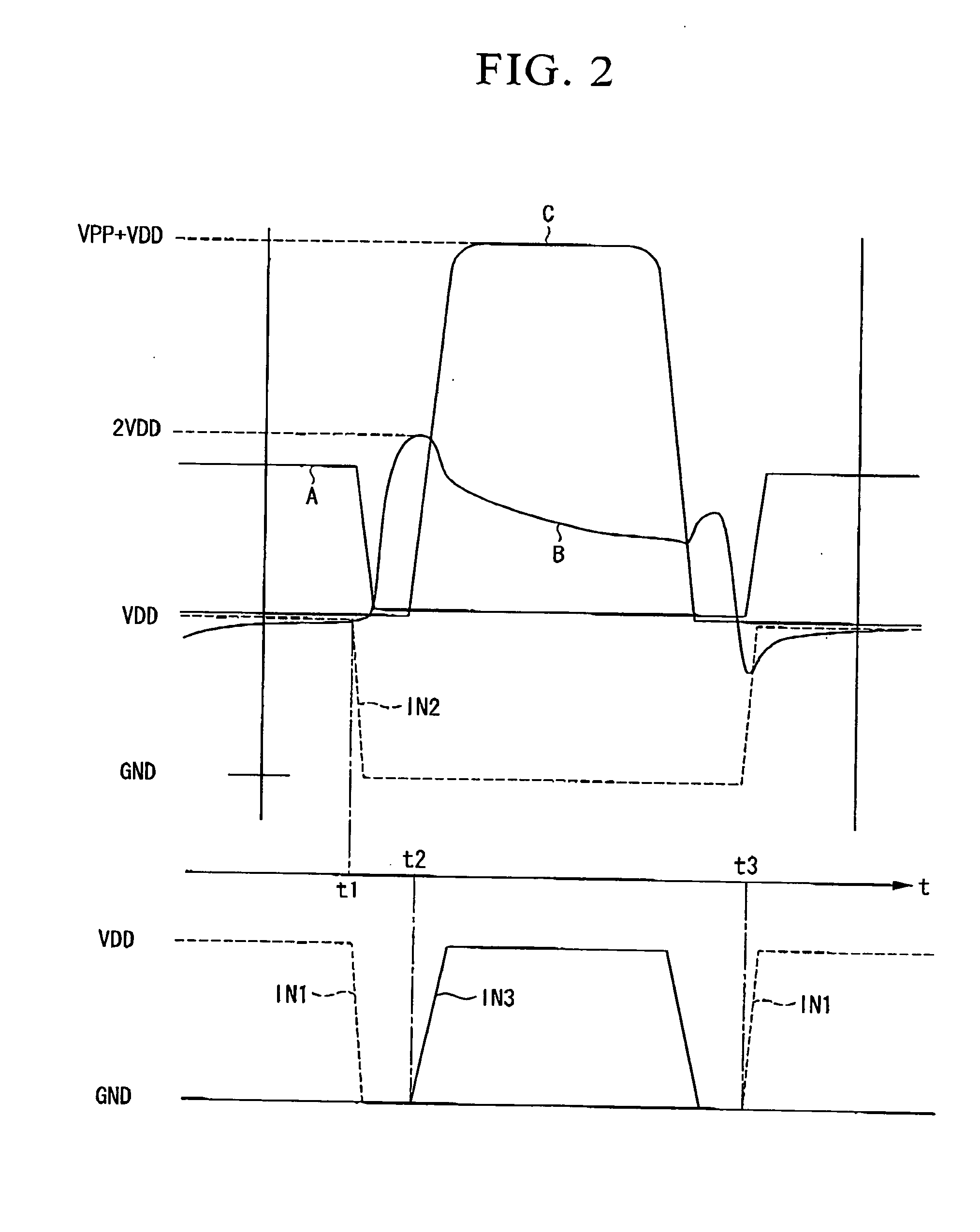
[0058]With regard to the charge pump unit 11 shown in FIG. 1, clock signals IN1, IN2 and IN3 have different phases. A clock signal generation portion 13 generates the clock signals IN1, IN2 and IN3. Transistors...
second embodiment
[0074](A Case of Being Applied to DDR2 Specifications)
[0075]FIG. 3 is a drawing which shows a constitution of a boosting charge pump circuit of a second embodiment. FIG. 1 shows an example of a boosting charge pump circuit which is applied with DDR2 specifications (for example, the power supply voltage is 1.8 V).
[0076]The boosting charge pump circuit shown in FIG. 3 is constituted from two charge pump circuit units 11A and 12A. Both the charge pump circuit units 11A and 12A are connected in serial so as to adjust the internal voltage VPP of the internal power line 21 in a range of “3×VDD>VPP>2×VDD”.
[0077]Constitutions of the charge pump circuit units 11A and 12A are substantially the same as the charge pump circuit units 11 and 12 respectively shown in FIG. 1. Connection statuses of the wiring of the connection switching terminals SW1-SW4 and SW1′-SW4′ are partially different between the charge pump circuit units 11A / 12B and 11 / 12.
[0078]With regard to the above-described differences...
third embodiment
[0094]FIG. 5 is a drawing which shows a constitution of a boosting charge pump circuit of a third embodiment.
[0095]In the boosting charge pump circuit shown in FIG. 5, constitutions of the charge pump circuit units 11B and 12B are substantially the same as the charge pump circuit units 11 and 12 respectively shown in FIG. 1 which satisfies DDR1 specifications.
[0096]The following points of the boosting charge pump circuit shown in FIG. 5 are different form the boosting charge pump circuit shown in FIG. 1. An NMOS transistor M5 is inserted between the point B at which the capacitor C2 of the charge pump circuit unit 11B is connected and the point B′ at which the capacitor C2′ of the charge pump circuit unit 12B is connected. Moreover, a clock signal IN4, a connection switching terminal SW5 and a buffer gate G4 are added. It should be noted that, with regard to the buffer gate G4, the supply source voltage (circuit voltage) is the internal voltage VPP. Moreover, the clock signal genera...
PUM
 Abstract
Description
Claims
Application Information


