Method of Fabricating Semiconductor Device, and Developing Apparatus Using the Method

a technology of semiconductor devices and developing apparatus, which is applied in the direction of photomechanical equipment, instruments, photosensitive material processing, etc., can solve the problems of resist pattern sidewall angle becoming difficult to measure accurately, resist removal becoming difficult, and sidewall angle becoming rounded

Inactive Publication Date: 2008-07-31
SEMICON ENERGY LAB CO LTD
View PDF5 Cites 8 Cited by
  • Summary
  • Abstract
  • Description
  • Claims
  • Application Information

AI Technical Summary

Benefits of technology

[0032]According to the invention constructed in the above-described manner, the irradiation of a developed resist pattern with light of wavelength 350-450 nm which is light within the range of photosensitive wavelengths of a DNQ photosensitizer is considered to provide the action of lowering the glass transition temperature of the resist pattern and the action of promoting the solubility in a resist removing solution of the resist pattern except the surface portion of the resist pattern after dry etching processing (i.e., a deteriorated layer portion formed during dry etching). Accordingly, when a resist pattern is to be baked at a temperature not lower than the glass transition temperature of the resist pattern, it is possible to realize a decrease in a bake temperature for obtaining the desired sidewall angle of the resist pattern. In the case where the bake temperature is not decreased, the sidewall angle of the resist pattern can be smaller owing to the promotion of softening and fluidization. This fact means that in a taper etching process based on a resist-receding method, a taper portion can be formed to have a far longer size. In addition, in the processing of removing a resist pattern after dry etching processing, it is possible to completely remove the resist pattern without leaving resist residues, through an ashing step and a resist removing step. Therefore, the semiconductor device fabricating method to which the invention is applied is extremely advantageous for improving the process margin of the taper etching step based on the resist-receding method and for improving resist removability.
[0035]According to the invention constructed in the above-described, it is possible to perform continuous processing which includes developing processing, light irradiation processing for irradiating a developed resist pattern with light within the range of photosensitive wavelengths of a DNQ photosensitizer, and bake processing for baking the resist pattern at a temperature not lower than the glass transition temperature of the resist pattern. Accordingly, it is possible to positively realize a high-throughput process which satisfies the formation of a resist pattern having the desired sidewall angle (for example, not greater than 50 degrees) and the resist removability of the resist pattern.

Problems solved by technology

Incidentally, when the correlation data shown in FIG. 11B is to be acquired, the sidewall angle of the resist pattern is varied by performing bake processing at a temperature not lower than the glass transition temperature of the resist pattern, but the sidewall angle becomes rounded and the sidewall angle of the resist pattern becomes difficult to measure accurately.
It is known, however, that an increase in bake temperature leads to the problem that resist removal becomes difficult.
It has been experientially discovered that when bake processing on the resist pattern is performed at a temperature not lower than 170° C., the speed of ashing, although it depends on the kind of resist material, becomes slower and resist removability extremely deteriorate particularly in the resist removing step.
Accordingly, in the case of the resist pattern forming method of baking a resist pattern at a temperature not lower than the glass transition temperature of the resist pattern for the purpose of obtaining the desired sidewall angle (for example, not greater than 50 degrees) of the resist pattern, the problem that a process margin for resist removability cannot be ensured becomes apparent, with the result that it becomes difficult to compatibly realize both the formation of a resist pattern having the desired sidewall angle and the resist removability of the resist pattern.

Method used


Image

  • Method of Fabricating Semiconductor Device, and Developing Apparatus Using the Method
  • Method of Fabricating Semiconductor Device, and Developing Apparatus Using the Method
  • Method of Fabricating Semiconductor Device, and Developing Apparatus Using the Method

Examples


embodiment 1

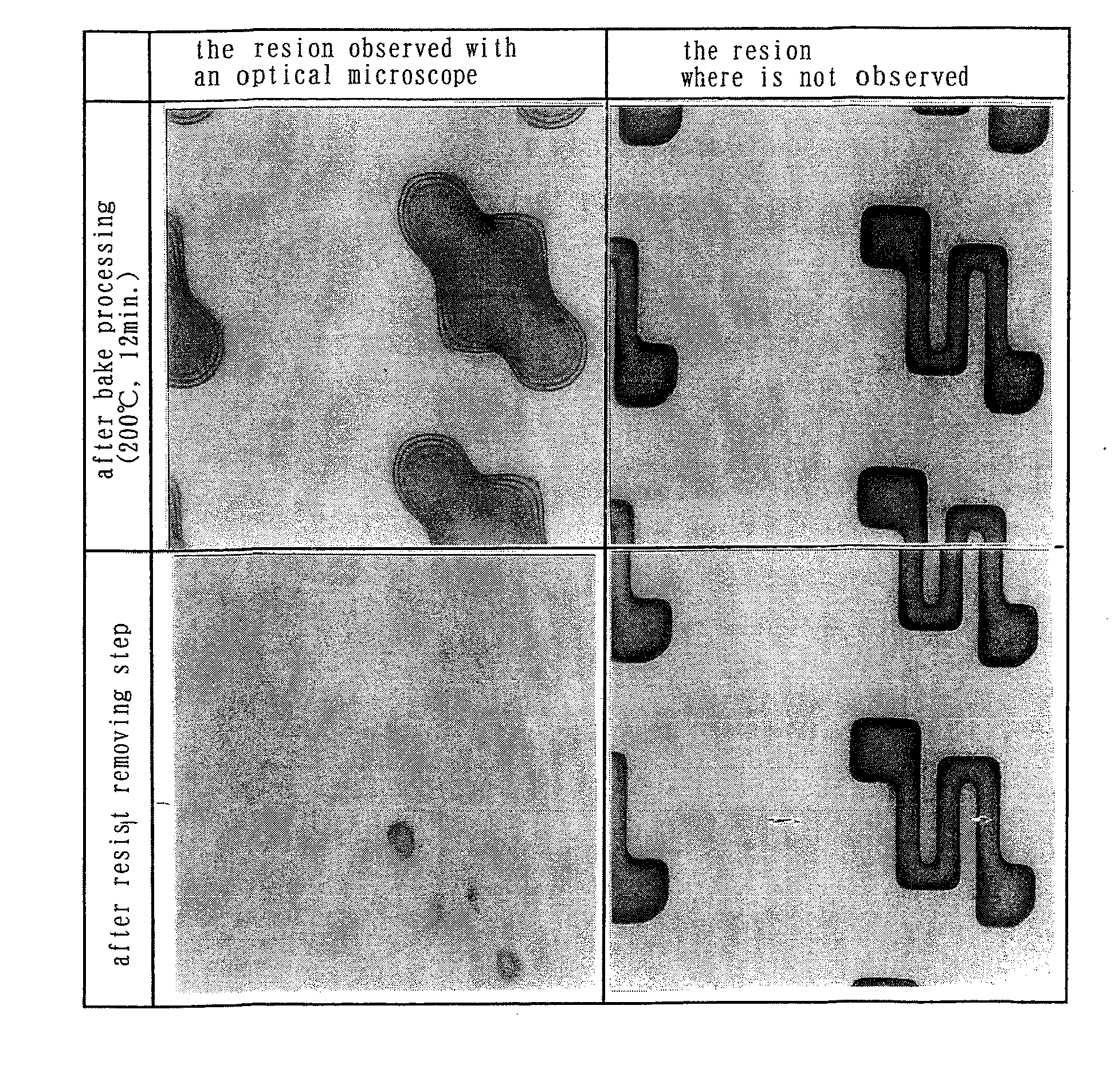
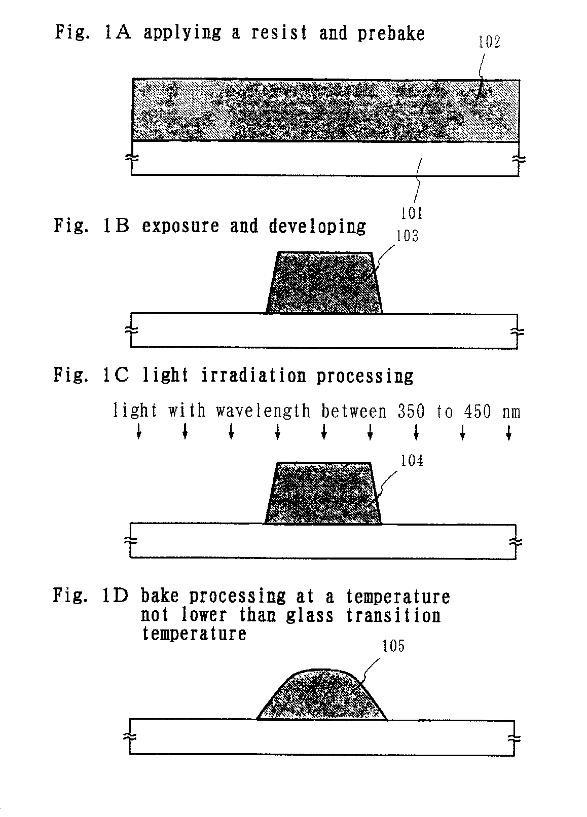
[0053]A resist pattern forming method according to Embodiment 1 of the invention will be described below with reference to FIGS. 1A to 1D. FIGS. 1A to 1D are cross-sectional process diagrams showing the resist pattern forming method.

[0054]First, a DNQ-novolac resin type of positive resist which is generally applied to a semiconductor device fabricating process is formed with a predetermined film thickness on an insulating transparent glass substrate 101 by spin coating method. After that, a predetermined time of prebake processing at a processing temperature of approximately 100° C. is performed to evaporate the solvent contained in the formed resist film and form a stable resist film, thereby forming a resist film 102 of predetermined film thickness. At this time, since the film thickness of the resist film 102 influences the size of a resist pattern to be finally formed, the precise control of spin conditions for spin coating is needed (refer to FIG. 1A).

[0055]Then, a 1:1 projecti...

embodiment 2

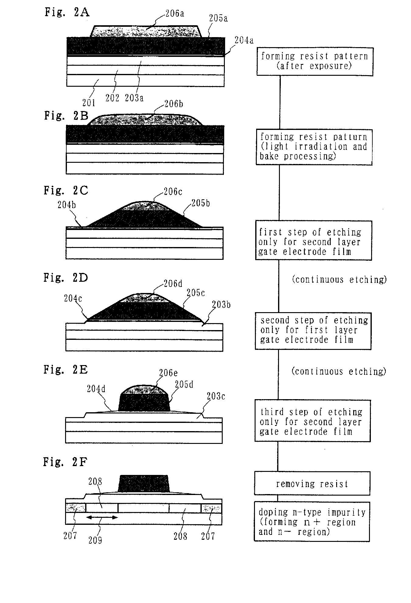
[0059]In the following description of Embodiment 2, based on FIGS. 2A to 2F, reference will be made to the case where the resist pattern forming method according to the invention is applied to a gate electrode forming process which includes a GOLD-structure TFT fabricating process. Incidentally, FIGS. 2A to 2F are cross-sectional process diagrams showing the GOLD-structure TFT fabricating process.

[0060]First, the structure of a substrate used in Embodiment 2 will be described. The shown substrate includes a glass substrate 201 which is an electrically insulating transparent substrate, and a base film (not shown) comprising a silicon oxide nitride film having a film thickness of 150 nm is deposited over the glass substrate 201, and a semiconductor layer which is a TFT active layer comprising a polycrystalline silicon film 202 having a film thickness of 50 nm is formed over the base film. A gate insulating film 203a comprising a silicon oxide film having a film thickness of 100 nm, a ...

embodiment 3

[0072]In the following description of Embodiment 3, a developing apparatus capable of performing continuous processing on the resist pattern forming process according to the invention will be described with reference to FIGS. 3 to 4. FIG. 3 is a schematic plan view showing the whole of the developing apparatus, and FIGS. 4A and 4B are cross-sectional views showing a specific construction of a light irradiation unit which constitutes a feature of the invention.

[0073]FIG. 3 is a schematic plan view showing the whole of the developing apparatus capable of performing continuous processing on the resist pattern forming process according to the invention, and shows a substrate-by-substrate processing type of developing apparatus 301 capable of continuously processing substrates to be processed one-by-one. The developing apparatus 301 includes a loader-side carrier 303 capable of accommodating a plurality of substrates 302 to be processed (generally, approximately twenty substrates), a plu...


PUM

PropertyMeasurementUnit
sidewall angleaaaaaaaaaa
temperatureaaaaaaaaaa
heightaaaaaaaaaa

Abstract

In a resist pattern forming method in which bake processing is performed at a temperature not lower than a glass transition temperature in order to obtain the desired sidewall angle, resist removable is difficult. Accordingly, in the resist pattern forming method of performing bake processing at a temperature not lower than a glass transition temperature, a process margin for resist removability cannot be ensured, so that there is the problem that it is impossible to compatibly realize both the formation of a resist pattern having the desired sidewall angle and the resist removability of the resist pattern. The invention aims to solve the problem. A resist pattern including a diazonaphthoquinone (DNQ)-novolac resin type of positive resist is formed, and the resist pattern is irradiated with light within the range of photosensitive wavelengths of a DNQ photosensitizer to perform bake processing on the resist pattern at a temperature not lower than the glass transition temperature of the resist pattern.

Description

BACKGROUND OF THE INVENTION[0001]1. Field of the Invention[0002]The present invention relates to a method of fabricating a semiconductor device and, more particularly, to a method of forming a resist pattern in a photolithography process. The invention further relates to a developing apparatus using the fabrication method. Incidentally, the term “semiconductor device” used herein generally represents a semiconductor device of the type which has a circuit construction made of thin film transistors (hereinafter abbreviated to TFTs), and display devices such as an active matrix type liquid crystal display device or an EL (abbreviation for Electroluminescence) display device are included in the category of the semiconductor device.[0003]2. Description of the Related Art[0004]In recent years, active matrix types of liquid crystal display devices having circuit constructions including TFTs are applied to the display screens of personal computers and television sets, and various products a...

Claims


Application Information

Patent Timeline
Patent Type & Authority Applications(United States)
IPC IPC(8): G03F7/26G03F7/40H01L21/027H01L21/3213H01L21/336H01L21/77H01L21/84H01L27/12H01L29/423H01L29/49H01L29/786
CPCG03F7/40H01L21/0273H01L21/32136H01L21/32139H01L27/1214H01L27/1288H01L29/4908H01L29/66757H01L29/78621H01L29/78675H01L29/42384
Inventor NAGAI, MASAHARUUEHARA, ICHIRO
Owner SEMICON ENERGY LAB CO LTD
Why Eureka
Try Eureka