Nonvolatile semiconductor memory and method of access evaluation to the same
- Summary
- Abstract
- Description
- Claims
- Application Information
AI Technical Summary
Benefits of technology
Problems solved by technology
Method used
Image

Examples
first embodiment
The First Embodiment
Circuitry
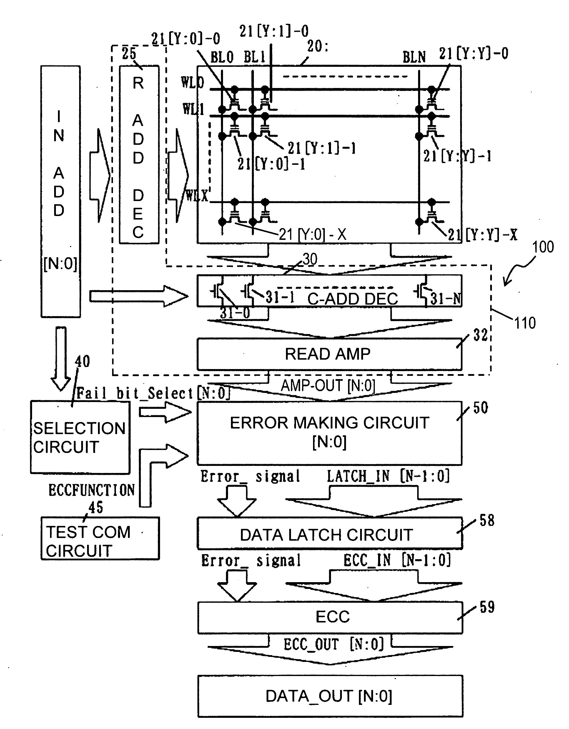
[0035]FIG. 1 is a circuit diagram of an asynchronous nonvolatile semiconductor memory 100 (as described above, hereinafter called “a nonvolatile memory”) having an error correcting function, such as an EPROM, according to the first embodiment. The nonvolatile memory 100 includes a memory cell array 20 for storing data. The memory cell array 20 includes a plurality of word lines WL (WL0˜WL127) and a plurality of bit lines BL (BL0˜BL127), each of which is perpendicular to the word lines WL. Although it is defined in the first embodiment that the number of the word lines WL is set at 128, which includes one hundred twenty seven (127) word lines for a data bits, and one word line for parity bit, and the number of the bit lines BL is set at 128, which includes one hundred twenty seven (127) bit lines for data bits, and one bit line for parity bit, the number of the word lines and the number of the bit lines can be changed. Namely, it can be described that the...
second embodiment
The Second Embodiment
[0054]The second embodiment is explained as follows with reference to FIG. 7˜FIG. 9. FIG. 7 is a circuit diagram of an asynchronous nonvolatile semiconductor memory having an error correcting function, according to the second embodiment. As described above, in each drawing and in each embodiment, the same reference numbers used in FIGS. 7˜9 designate the same or similar components used in the first embodiment.
[Circuitry]
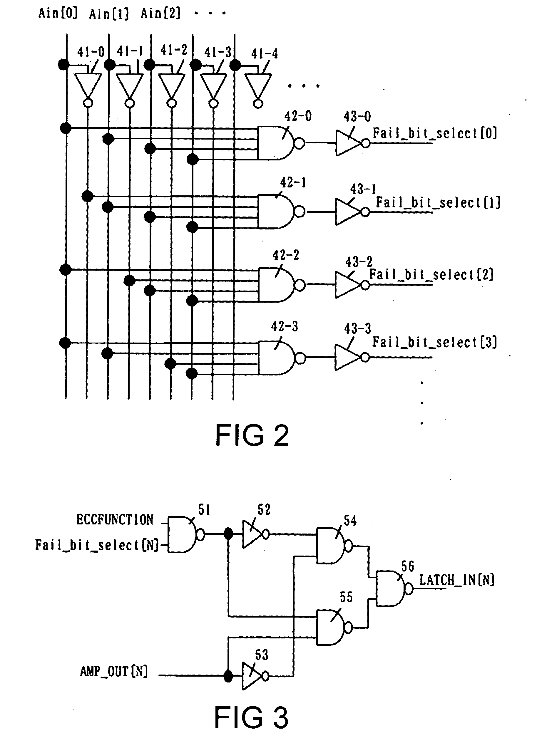
[0055]In the first embodiment, since the error making circuits 50 for making a one-bit error is formed between the read AMP 32 and the data latch circuit 58, the amplified signal AMP_OUT [N:0] under the general operation is also required to pass through the error making circuit 50 in order to be reached to the data latch circuit 58. Thus, the amplified signal AMP_OUT [N:0] may not be held in the data latch circuit 58 stably.
[0056]According to the second embodiment, a plurality of error making circuits 50A, each of which has the same components as...
third embodiment
The Third Embodiment
[0066]According to the nonvolatile memories 100 and 200 of the first and the second embodiment shown in FIG. 1 and FIG. 7, since the selection circuit 40 used in either nonvolatile memory 100 or 200 can select the desired one of the memory cells, it is possible to evaluate the delay caused by the arithmetic operation for one-bit correction to the single data group (for example, 128-bit data [127:0]-0 are considered as a single data group where Y=128 in the memory cells 21[Y:0]-0˜21[Y:Y]-0 whose gates are connected to the word line WL0). However, under such a method of the access evaluation, the operation for correcting one-bit error is performed one-hundred twenty eight (128) times to the single data group. Thus, the delay testing time for correction takes 128 times longer, and the scale of the circuit increases.
[0067]According to the third embodiment, in order to reduce the testing time and the scale of the circuit, an all-bit rescuing test is not performed for ...
PUM
 Abstract
Description
Claims
Application Information
 - R&D Engineer
- R&D Manager
- IP Professional
- Industry Leading Data Capabilities
- Powerful AI technology
- Patent DNA Extraction
Browse by: Latest US Patents, China's latest patents, Technical Efficacy Thesaurus, Application Domain, Technology Topic.
© 2024 PatSnap. All rights reserved.Legal|Privacy policy|Modern Slavery Act Transparency Statement|Sitemap