Method and system for conducting design explorations of an integrated circuit

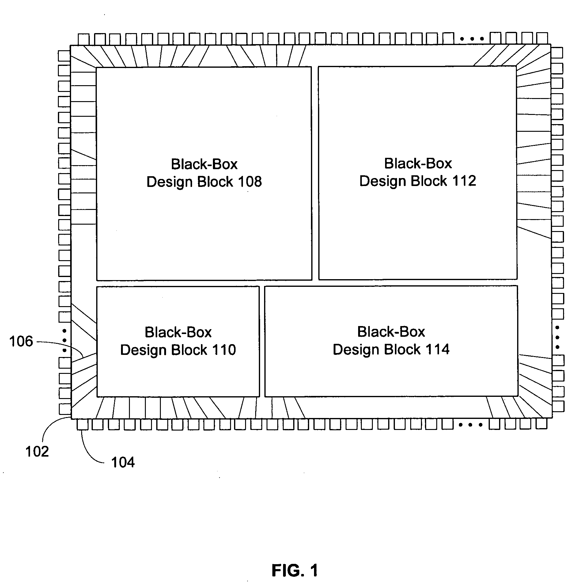
a technology of integrated circuits and design explorations, applied in the field of electronic design automation tools, can solve the problems of multiple modification of shapes or pin locations of black-box design blocks, shortening the development cycle of socs, and affecting the efficiency of early-stage design explorations, so as to improve the accuracy of design and increase the overall user productivity

Active Publication Date: 2008-07-31
CADENCE DESIGN SYST INC
View PDF4 Cites 13 Cited by
  • Summary
  • Abstract
  • Description
  • Claims
  • Application Information

AI Technical Summary

Benefits of technology

[0009]The present invention generally relates to a method and system for conducting design explorations of an integrated circuit. In various embodiments described herein, the method removes the limitations imposed by the conventional method of hard black-box design block modeling, by using soft design models and their corresponding template cells that are combined with an interface timing model. The soft design models remove the need for the user to specify any shape or pin location information, and replace such information with a user-specified area for a soft design model. This area is used to drive automatic shaping and pin assignment that is designed to closely track the actual placement of a gate-level netlist of the black-box design block. This approach improves the accuracy of the design, and increases overall user productivity by eliminating the need for the user to specify detailed shapes and pin locations during design iterations of the design exploration process.

Problems solved by technology

In addition to more complexity, consumers continue to demand faster time-to-market for such electronic devices, which lead to shorter development cycles for SoCs.
These circuit components are often referred to as hard-macros or hard physical models because they require fixed shape, pin locations, or routing obstruction information, which hinders the efficiency of early-stage design explorations as will be explained below.
One of the problems of the conventional design exploration using black-box design blocks is that the shapes or pin locations of the black-box design blocks are modified multiple times, often manually, during the design iteration process.
This is due to the hard-macro nature of the conventional black-box design block, which has a fixed shape, fixed pin locations along the boundary of the block, and fixed routing obstructions over the block.
In other words, since many design exploration iterations require some number of black-boxes to be reshaped and pins to be reassigned, some of the efforts put into the previous iteration of the design are wasted.
This process is inefficient and time consuming.

Method used


Image

  • Method and system for conducting design explorations of an integrated circuit
  • Method and system for conducting design explorations of an integrated circuit
  • Method and system for conducting design explorations of an integrated circuit

Examples


Embodiment Construction

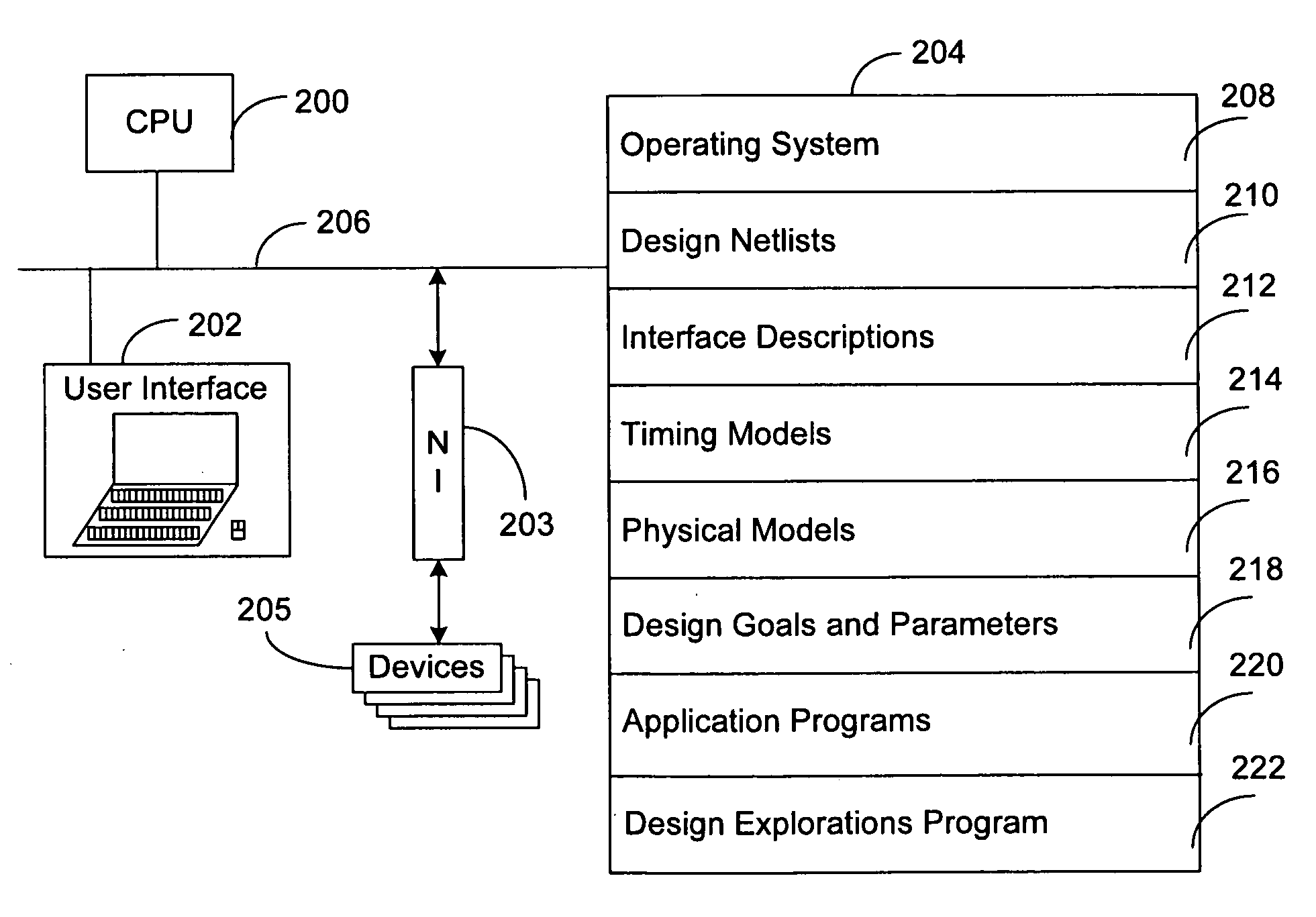
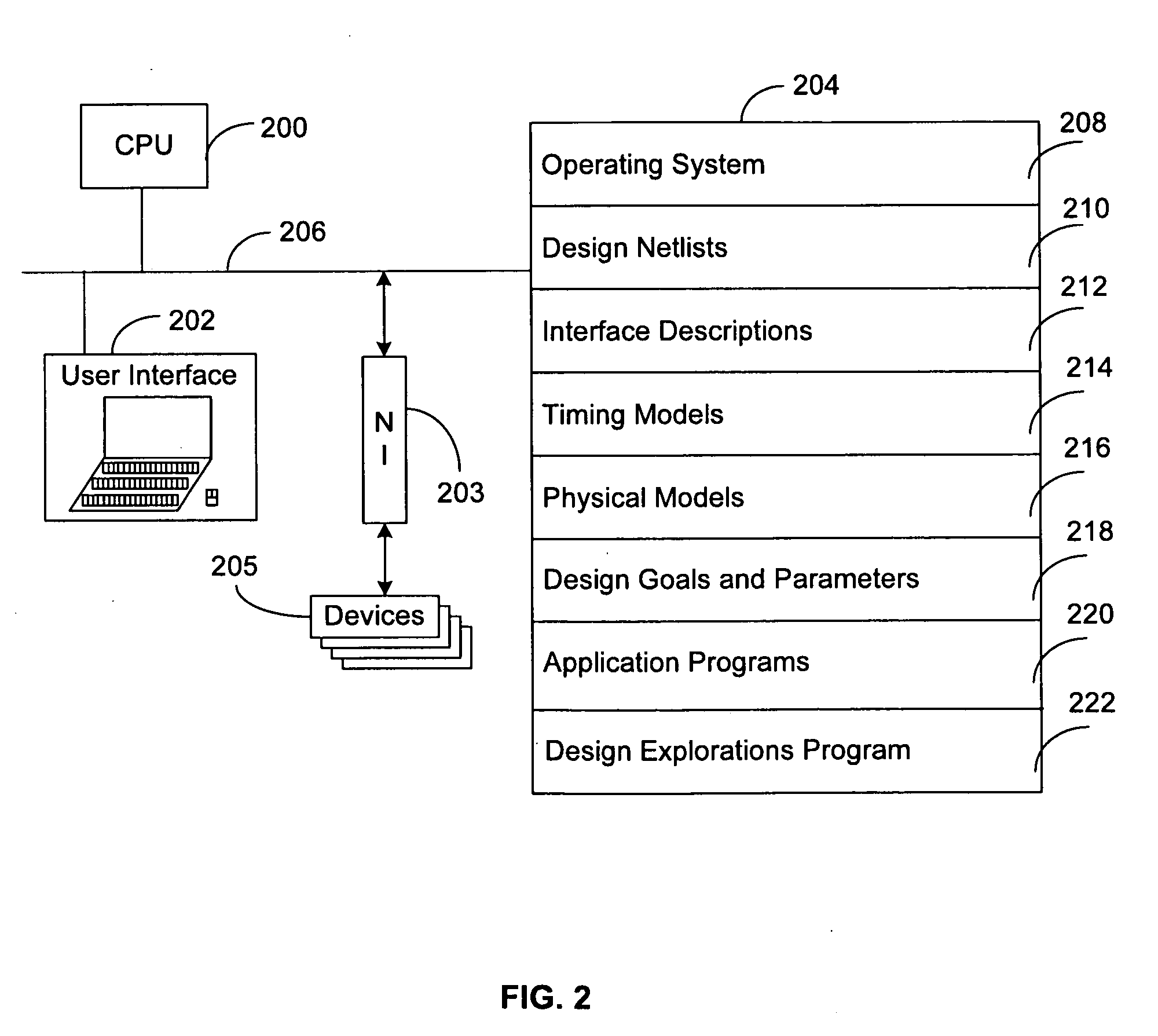
[0018]Methods and systems are provided for conducting design explorations of an integrated circuit. The following descriptions are presented to enable any person skilled in the art to make and use the invention. Descriptions of specific embodiments and applications are provided only as examples. Various modifications and combinations of the examples described herein will be readily apparent to those skilled in the art, and the general principles defined herein may be applied to other examples and applications without departing from the spirit and scope of the invention. Thus, the present invention is not intended to be limited to the examples described and shown, but is to be accorded the widest scope consistent with the principles and features disclosed herein.

[0019]Some portions of the detailed description that follows are presented in terms of flowcharts, logic blocks, and other symbolic representations of operations on information that can be performed on a computer system. A pr...


PUM


Abstract

Method and system for conducting design explorations of an integrated circuit are disclosed. In one embodiment, the method includes obtaining a design description of the integrated circuit that includes a virtual design block, creating a representative netlist for representing the virtual design block, where the representative netlist includes one or more soft design models, and each soft design model comprises one or more template cells for modeling a portion of the integrated circuit. The method further includes defining physical attributes for the one or more soft design models in accordance with area requirements of the virtual design block, where the one or more soft design models are described with flexible shape and pin locations, performing design explorations of the integrated circuit using the one or more soft design models and their corresponding template cells, and generating a representative implementation of the integrated circuit using results of the design explorations.

Description

FIELD OF THE INVENTION[0001]The present invention relates to the field of electronic design automation tools. In particular, the present invention relates to a method and system for conducting design explorations of an integrated circuit.BACKGROUND OF THE INVENTION[0002]In recent years, consumer electronic devices, such as cellular phones, digital cameras, MP3 players, and personal digital assistant (PDA) devices, have had significant success in the marketplace. The compact design of such consumer electronic devices requires more and more functionalities to be packed into one integrated circuit chip, also referred to as system-on-chip (SoC). In response to this market demand, new semiconductor processing technologies, such as the 90 nm and 65 nm processing technologies, have made it feasible to place millions of logic gates on a single integrated circuit. With such processing technologies, functional blocks such as the central processing unit (CPU), memory, graphic applications, com...

Claims


Application Information

Patent Timeline
Patent Type & Authority Applications(United States)
IPC IPC(8): G06F17/50
CPCG06F17/5068G06F17/5045G06F30/39G06F30/30
Inventor MCCRACKEN, THADDEUS CLAYLEE, JONG-CHANGWU, PING-CHIHNGHIEM, CECILECHEONG, KIT LAMEICHENSEER, PATRICK JOHN
Owner CADENCE DESIGN SYST INC
Why Eureka
Try Eureka