Method for performing monte-carlo simulations to predict overlay failures in integrated circuit designs

Inactive Publication Date: 2005-05-10
IBM CORP
View PDF7 Cites 15 Cited by
  • Summary
  • Abstract
  • Description
  • Claims
  • Application Information

AI Technical Summary

Benefits of technology

[0011]It is another object of the present invention to provide a method for improving integrated circuit design accuracy.
[0012]A further object of the invention is to provid

Problems solved by technology

Each step in the manufacturing process introduces a certain amount of error, which causes the final resulting manufactured chip pattern design to deviate somewhat from that originally provided by the designer.
Some of the places where errors are introduced are: 1) imperfections in the physical realization of the photo mask, 2) shape image distortion in the lithographic process used to expose wafers, 3) variations in the process across a single chip and/or wafer, 4) variations in the process from wafer to wafer, and 5) misalignment of photo masks from adjacent layers (overlay error).
In other cases, the imperfections lead to some conservatism in the design process.
In reality, however, certain geometries or configurations or circuit portions are much more susceptible to failure than others.
However, the same foreshortening becomes of greater concern if that foreshortening, combined with other process imper

Method used


Image

  • Method for performing monte-carlo simulations to predict overlay failures in integrated circuit designs
  • Method for performing monte-carlo simulations to predict overlay failures in integrated circuit designs
  • Method for performing monte-carlo simulations to predict overlay failures in integrated circuit designs

Examples


Example

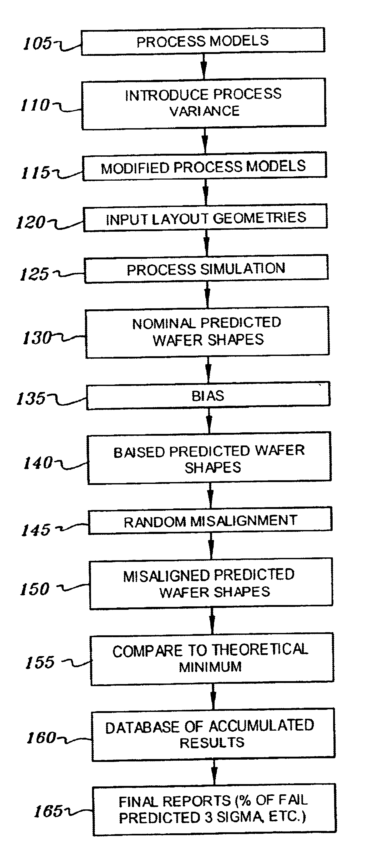
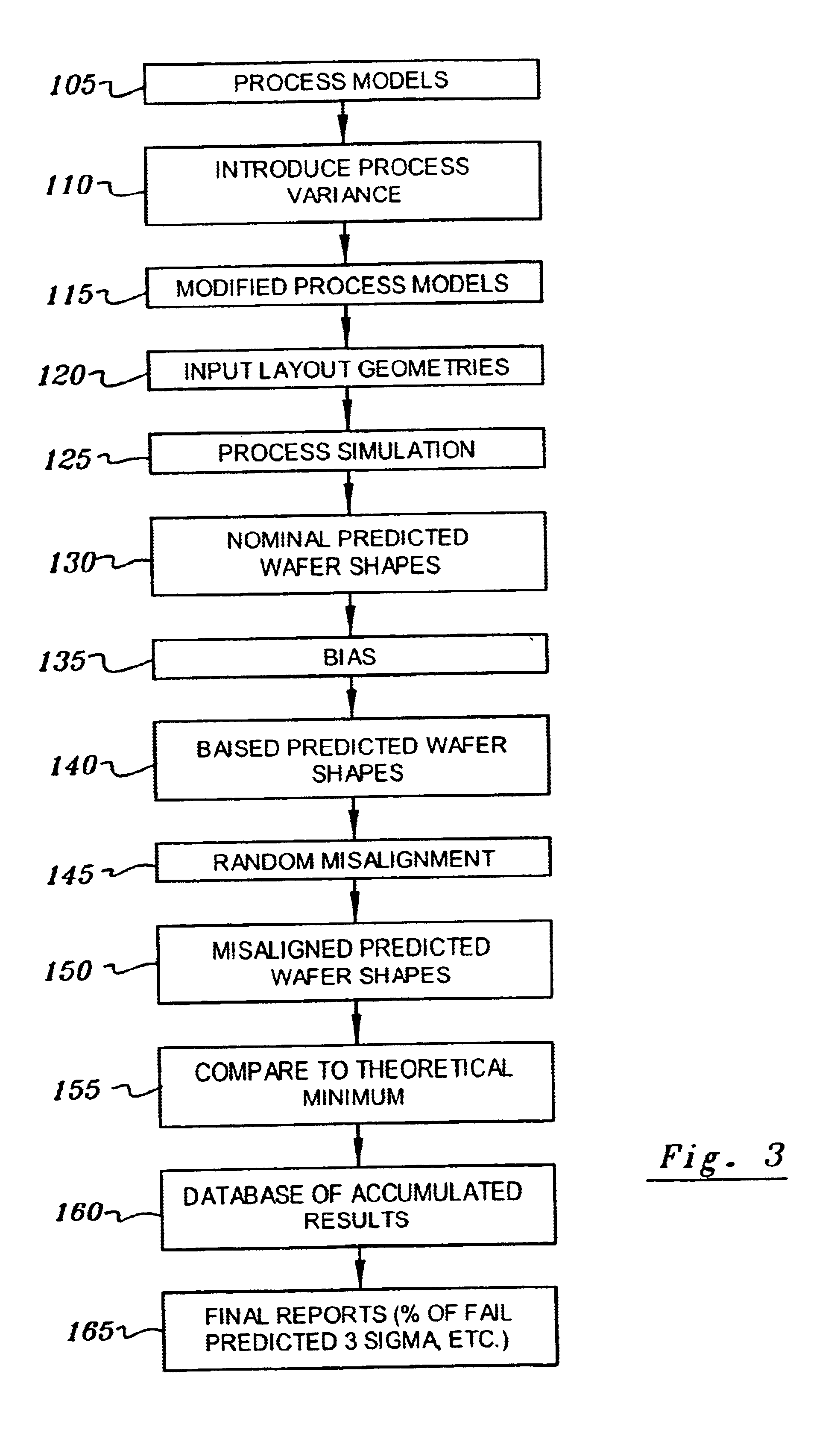
[0028]In describing the preferred embodiment of the present invention, reference will be made herein to FIGS. 1-6 of the drawings in which like numerals refer to like features of the invention. Features of the invention are not necessarily shown to scale in the drawings.

[0029]The present invention provides a method for gathering statistics as to, and predicting, the susceptibility of failure of specific geometries on one or more physically adjacent layers in a circuit design with respect to variations in the manufacturing process. The method involves the performing of monte-carlo simulations specific to a given technology, and introduction of random variation for both overlay error and the process itself.

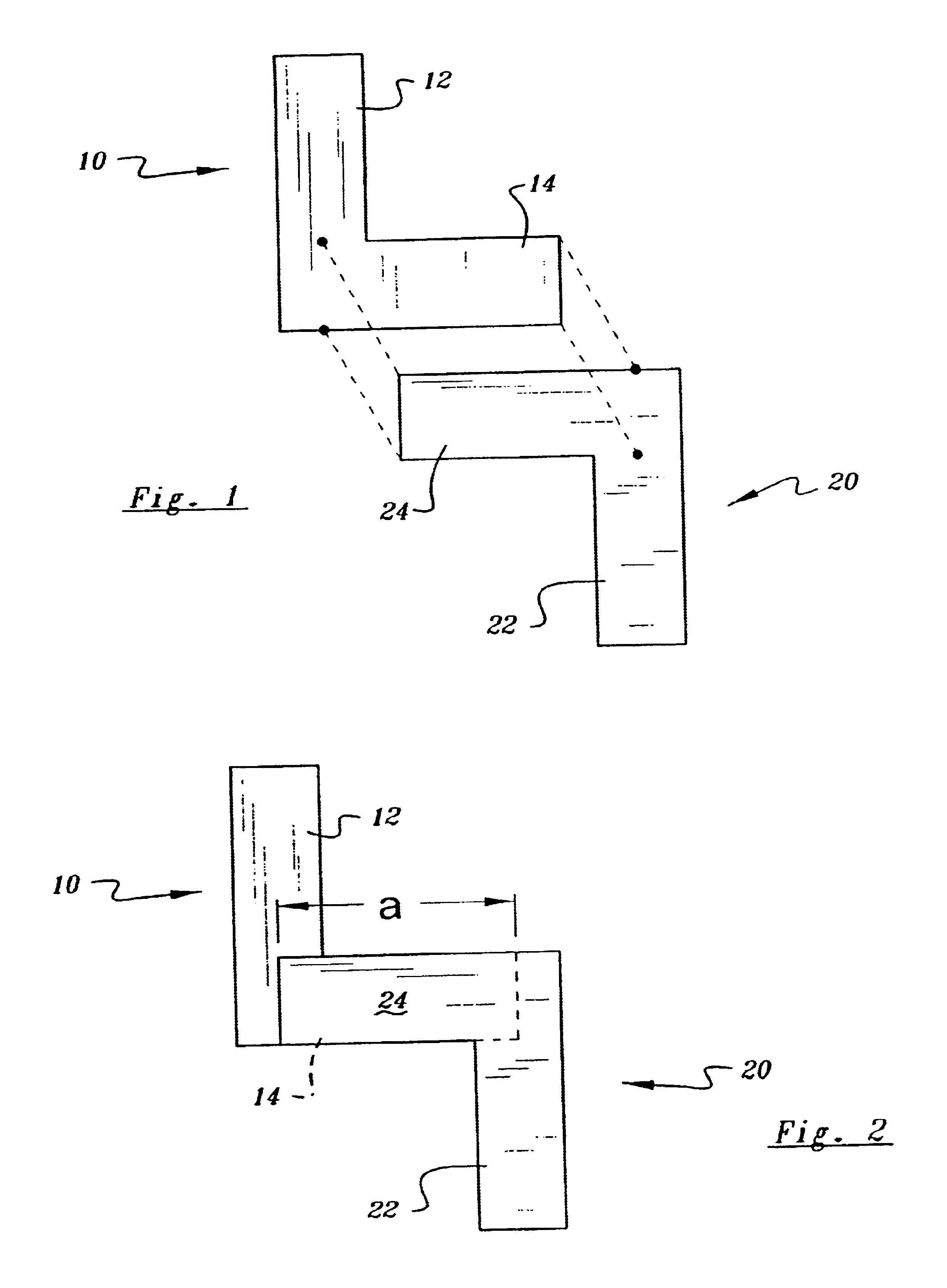
[0030]FIG. 1 shows ideal portions of an integrated circuit configuration, as designed, which are intended to be formed on adjacent layers of a semiconductor wafer. Designed circuit portion 10 to be formed on a first wafer layer consists of, for example, a metal deposition having a f...


PUM


Abstract

A method of predicting overlay failure of circuit configurations on adjacent, lithographically produced layers of a semiconductor wafer comprises providing design configurations for circuit portions to be lithographically produced on one or more adjacent layers of a semiconductor wafer, and then predicting shape and alignment for each circuit portions on each adjacent layer using one or more predetermined values for process fluctuation or misalignment error. The method then determines dimension of overlap of the predicted shape and alignment of the circuit portions, and compares the determined dimension of overlap to a theoretical minimum to determine whether the predicted dimension of overlap fails. Using different process fluctuation values and misalignment error values, the steps are then iteratively repeated on the provided design configurations to determine whether the predicted dimension of overlap fails, and a report is made of the measure of failures.

Description

BACKGROUND OF INVENTION[0001]This invention relates to the lithographic production of integrated circuits and, in particular, to a method of predicting overlay failure of circuit configurations on adjacent, lithographically produced layers of a semiconductor wafer.[0002]The integrated circuit fabrication process consists of a series of steps which begins with an input set of geometries or configurations of integrated circuit patterns provided by the very large scale integration (VLSI) designer and results in a manufactured integrated circuit chip consisting of devices and interconnects which perform a needed function. Exposure tools print the integrated circuit patterns by lithographic methods on successive layers of a semiconductor wafer. These lithographic methods are well known and include using a photo mask to project the image of the circuit portion onto a resist layer, developing the resist layer, removing portions of the resist layer to recreate the circuit portion image on t...

Claims


Application Information

Patent Timeline
IPC IPC(8): G06F17/50H01L21/02H01L21/027
CPCG06F17/5081G06F30/398
Inventor CULP, JAMES A.LAVIN, MARK A.SAYAH, ROBERT T.
Owner IBM CORP
Why Eureka
Try Eureka