Flim type package for fingerprint sensor

a fingerprint sensor and packaging technology, applied in solid-state devices, instruments, semiconductor devices, etc., can solve the problems of inability to implement existing packaging processes and equipment, damage to fingerprint sensor chips or other components, and static electricity to come along and accumula

Active Publication Date: 2008-08-07
CHIPMOS TECH INC
View PDF12 Cites 24 Cited by
  • Summary
  • Abstract
  • Description
  • Claims
  • Application Information

AI Technical Summary

Benefits of technology

[0006]The main purpose of the present invention is to provide a thin-film fingerprint sensor package where the static electricity, caused by sliding the fingers during fingerprint recognition, can be safely discharged by a ground lead of a wiring film electrically connecting the chip to the metal base to achieve the protection of electrostatic discharge, ESD, and to avoid the fingerprint sensor chip from damages.

Problems solved by technology

However, when sliding the fingers for fingerprint recognitions, static electricity will come along and accumulate in the fingerprint sensor package.
When static electricity is discharged, the fingerprint sensor chip or the other components will be damaged.
However, there is a risk of contamination of the sensing area during encapsulation, moreover, the existing packaging processes and equipment can not be implemented.

Method used


Image

  • Flim type package for fingerprint sensor
  • Flim type package for fingerprint sensor
  • Flim type package for fingerprint sensor

Examples


first embodiment

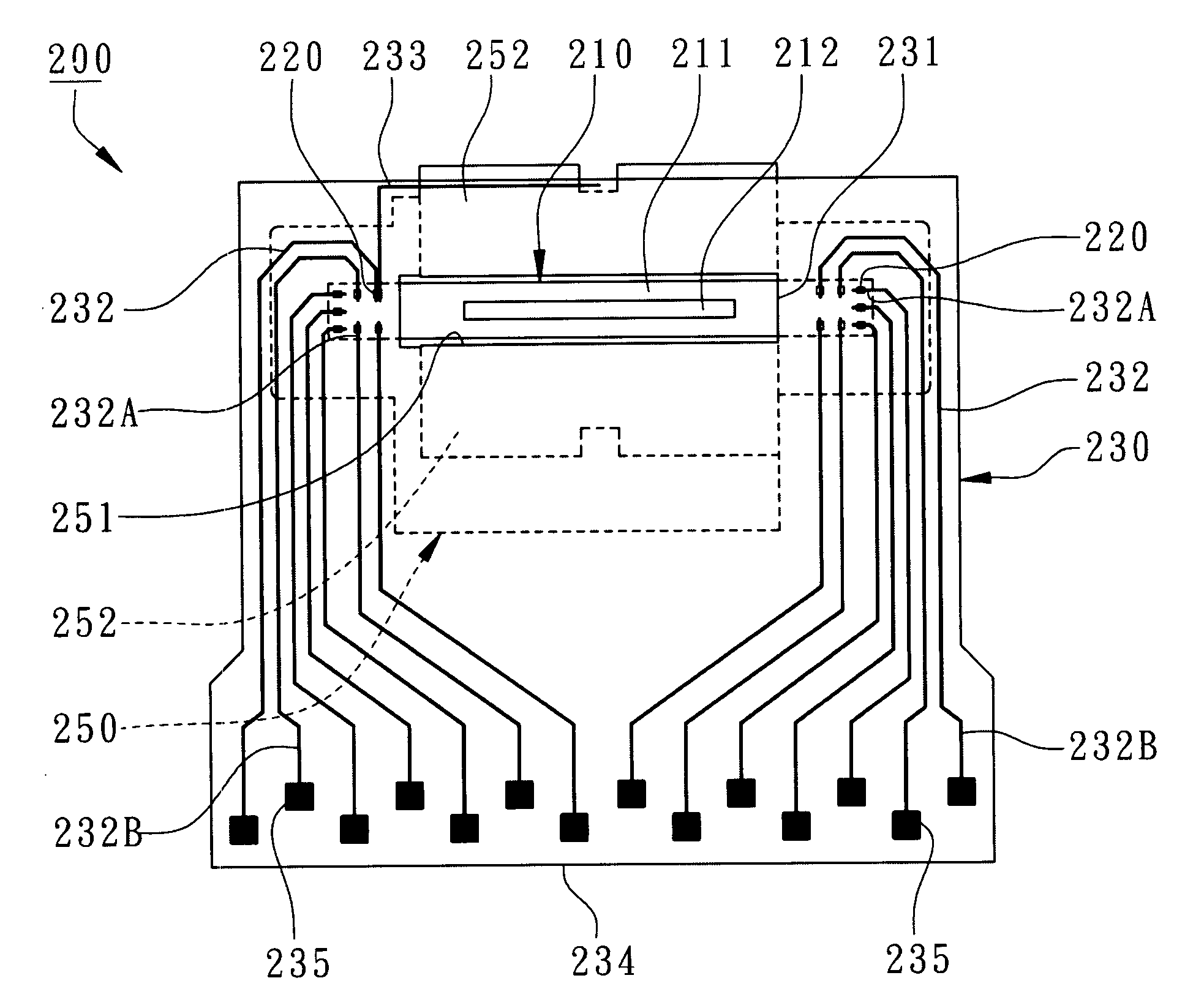
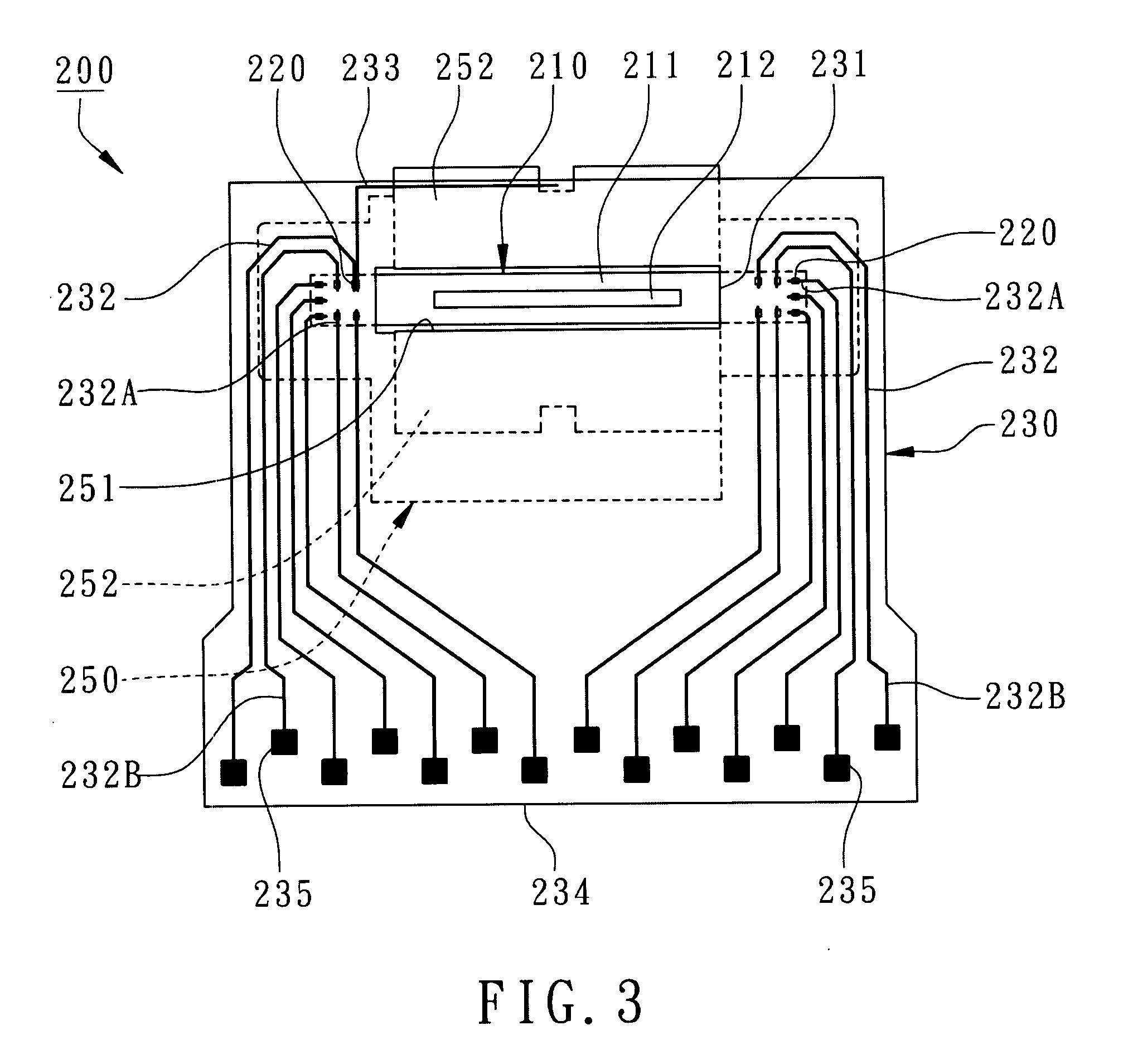
[0015]According to the present invention, as shown in FIG. 3 and FIG. 5, a thin-film fingerprint sensor package 200 primarily comprises a fingerprint sensor chip 210, a plurality of bumps 220, a wiring film 230, an encapsulant 240 and a metal base 250 where the wiring film 230 is the chip carrier for the fingerprint sensor chip 210 during reel-to-reel packaging processes. The fingerprint sensor chip 210 is electrically connected to the wiring film 230 by the bumps 220 or / and the others, such as ACF (antisotropic conductive film) or NCP (non-conductive paste).

[0016]A sensing area 212 is formed on the active surface 211 of the fingerprint sensor chip 210. Normally, there are light-sensing components, RF sensing components, or sensing components which can sense pressures, temperatures, or capacitance formed in the sensing area 212 for fingerprint recognition. As shown in FIG. 3, the sensing area 212 is a strip or other shapes so that with fingers dynamically sliding or statically press...

second embodiment

[0025]According to the present invention, as shown in FIG. 6, another thin-film fingerprint sensor package 300 primarily comprises a fingerprint sensor chip 310, a plurality of bumps 320, a wiring film 330, an encapsulant 340, and a metal base 350. The fingerprint sensor chip 310 has a sensing area 312 included in the active surface 311, and the bumps 320 are disposed on the active surface 311.

[0026]The wiring film 330 has an opening 331 to expose the sensing area 312 where the wiring film 330 has a plurality of leads 332 and at least a ground lead 333. The inner ends 332A of the leads 332 and the inner ends 333A of the ground lead 333 are bonded to the corresponding bumps 320. In the present embodiment, the wiring film 330 can be parts of a TCP (Tape Carrier Package) tape where the inner leads 332A of the leads 332 and the inner leads 333A of the ground lead 333 are extended and suspended over the slot 331. The encapsulant 340 encapsulates the bumps 320. The fingerprint sensor chip...


PUM


Abstract

A thin-film fingerprint sensor package primarily comprises a fingerprint sensor chip, a plurality of bumps, a wiring film, an encapsulant and a metal base to mechanically hold the fingerprint sensor chip. A sensing area is formed on the active surface of the fingerprint sensor chip. The bumps are disposed on the active surface. The wiring film has an opening to expose the sensing area and comprises a plurality of leads bonded to the bumps. The wiring film further has a ground lead electrically connecting the fingerprint sensor chip to the metal base. Therefore, the fingerprint sensor package can provide ESD protection during fingerprint recognition to avoid the damage of the fingerprint sensor chip.

Description

FIELD OF THE INVENTION[0001]The present invention relates to a fingerprint sensor package, especially, to a film-type fingerprint sensor package.BACKGROUND OF THE INVENTION[0002]There are many electronic devices to enhance our working efficiencies every day such as cellular phones, notebook computers, personal digital assistants (PDA), etc. Since the competitions among the same businesses are getting intense, trade secrets have drawn many attentions these days. Therefore, there are more and more electronic devices have included security screening devices such as fingerprint sensors to ensure the trade secrets will not be leaked out to the opponents, and only the owners of the electronic devices can initiate the electronic devices and access to the information inside the electronic devices through the scanning of their fingerprints. Moreover, with the fingerprint sensors added to these electronic devices, the market values of these electronic devices will be higher.[0003]So far finge...

Claims


Application Information

Patent Timeline
Patent Type & Authority Applications(United States)
IPC IPC(8): G06K9/00
CPCG06K9/00053H01L2224/48091H01L2224/73265H01L2924/15311H01L2924/1815H01L2924/00014G06V40/1329
Inventor HUANG, MING-LIANGLEE, YAO-JUNGLI, MING-HSUN
Owner CHIPMOS TECH INC
Why Eureka
Try Eureka