Test structure for seal ring quality monitor

a technology of quality monitor and test structure, which is applied in the direction of semiconductor/solid-state device testing/measurement, semiconductor device details, semiconductor/solid-state device testing/measurement, etc., can solve the problems of increasing the chances of crack formation, increasing the difficulty of maintaining yield and throughput, and prone to damage of low-k dielectric materials in dies

Active Publication Date: 2008-08-14
TAIWAN SEMICON MFG CO LTD
View PDF9 Cites 74 Cited by
  • Summary
  • Abstract
  • Description
  • Claims
  • Application Information

AI Technical Summary

Problems solved by technology

Along with these advancements, the challenges of maintaining yield and throughput have also increased.
With regard to reliability, the presence of low-k materials near die corners increases the chances of crack formations, especially in the sawing process.
A typical problem is that the low-k dielectric materials in dies are prone to damage incurred by stress introduced by the sawing process.
When cracks form in low-k dielectric materials, copper lines in the low-k dielectric materials may be damaged.
However, OM inspection is objective, and hence is unreliable.
Particularly, it is difficult to differentiate whether the damage is a backside chipping of the semiconductor die or an inter-metal dielectric (IMD) crack.
The backside chipping can be easily solved by adjusting the sawing process, while the cracking of low-k dielectric materials is a much harder issue to solve.
Without being able to reliably identify the root cause of the problem, it is hard to determine the action to be taken.

Method used


Image

  • Test structure for seal ring quality monitor
  • Test structure for seal ring quality monitor
  • Test structure for seal ring quality monitor

Examples


Embodiment Construction

[0016]The making and using of the presently preferred embodiments are discussed in detail below. It should be appreciated, however, that the present invention provides many applicable inventive concepts that can be embodied in a wide variety of specific contexts. The specific embodiments discussed are merely illustrative of specific ways to make and use the invention, and do not limit the scope of the invention.

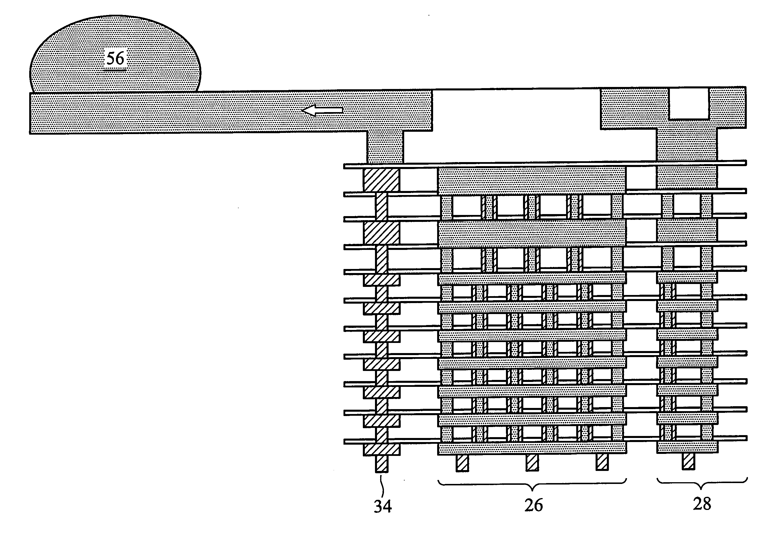
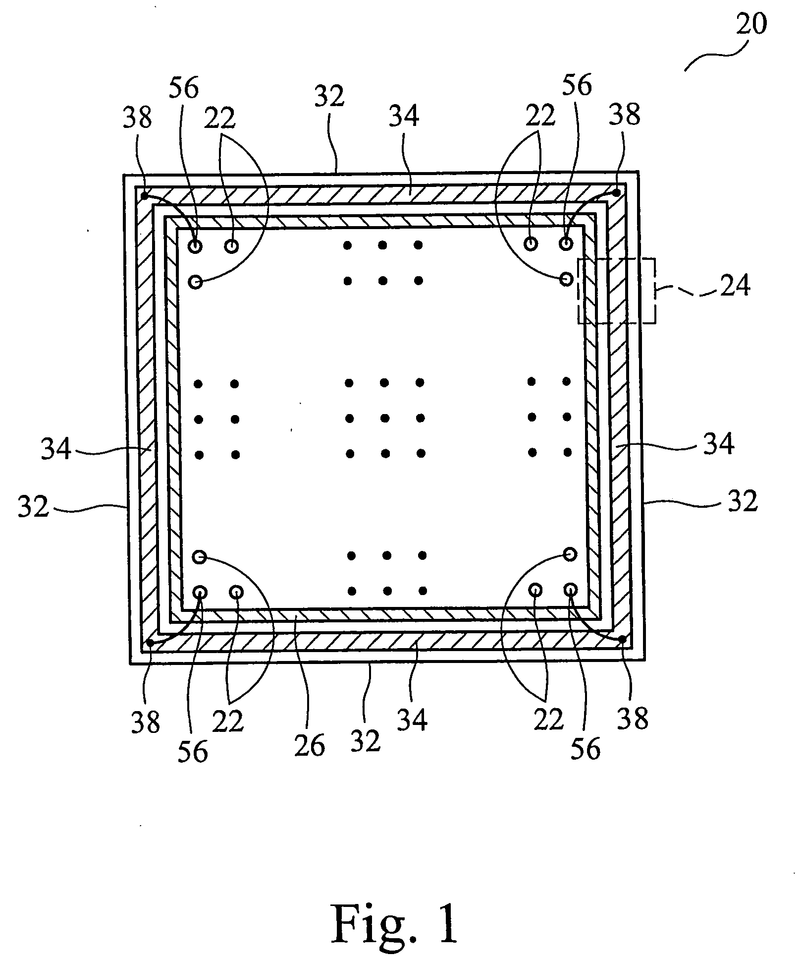
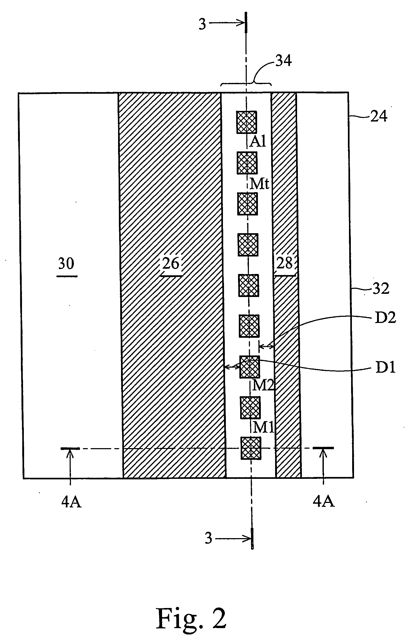
[0017]FIG. 1 illustrates a top view of semiconductor chip 20. A plurality of bumps 22 are formed on the top surface of semiconductor chip 20 and are connected to underlying circuits. Proximate edges 32 of semiconductor chip 20, seal ring 26, also referred to as main seal ring 26 throughout the description, are formed. As is known in the art, seal ring 26 forms a ring surrounding the integrated circuits in semiconductor chip 20, and is formed of metal lines and connecting vias. Since seal ring 26 is a tightly interconnected structure, it not only provides mechanical support to...


PUM


Abstract

A semiconductor structure includes a daisy chain adjacent to an edge of a semiconductor chip. The daisy chain includes a plurality of horizontal metal lines distributed in a plurality of metallization layers, wherein the horizontal metal lines are serially connected; a plurality of connecting pads in a same layer and electrically connecting the horizontal metal lines, wherein the connecting pads are physically separated from each other; and a plurality of vertical metal lines, each connecting one of the connecting pads to one of the horizontal metal lines, wherein one of the plurality of connecting pads is connected to one of the plurality of horizontal metal lines by only one of the plurality of vertical metal lines; and a seal ring adjacent and electrically disconnected from the daisy chain.

Description

TECHNICAL FIELD[0001]This invention relates to the manufacture of semiconductor chips having low-k dielectric materials, and more particularly to structures and methods for determining the quality of semiconductor chips.BACKGROUND[0002]Integrated circuits (IC) manufacturers are employing finer circuit widths, low dielectric constant (low-k) materials, and other technologies to make small, high-speed semiconductor devices. Along with these advancements, the challenges of maintaining yield and throughput have also increased. With regard to reliability, the presence of low-k materials near die corners increases the chances of crack formations, especially in the sawing process.[0003]A semiconductor wafer typically comprises isolated dies (or chips) separated from each other by scribe lines. Individual dies within the wafer contain circuitry, and the dies are separated by sawing. A typical problem is that the low-k dielectric materials in dies are prone to damage incurred by stress intro...

Claims


Application Information

Patent Timeline
Patent Type & Authority Applications(United States)
IPC IPC(8): H01L23/58
CPCH01L22/34H01L23/585H01L24/11H01L2224/48091H01L2924/00014H01L2224/0554H01L2224/05548H01L2224/05573H01L2224/05624H01L2224/05639H01L2224/05647H01L2224/05684H01L2224/0615H01L2924/14H01L2924/00H01L2224/05599H01L2224/0555H01L2224/0556H01L2224/45147
Inventor TSAI, HAO-YIHSU, SHIH-HSUNCHANG, SHIH-CHENGHOU, SHANG-YUNCHEN, HSIEN-WEITSAI, CHIA-LUNLIU, BENSONJENG, SHIN-PUUWU, ANBIARSHY
Owner TAIWAN SEMICON MFG CO LTD
Why Eureka
Try Eureka