

Thin film transistor device, method of manufacturing the same, and display apparatus
a transistor and thin film technology, applied in the field of thin film transistor devices, can solve the problems of increasing the damage difficult to completely etch the insulating film to form contact holes, and the failure to connect the bottom of the contact hole and the polysilicon film, so as to improve the withstand voltage of the gate insulating film, reduce leakage, and stable the capacitance of the storage capacitor
- Summary
- Abstract
- Description
- Claims
- Application Information
AI Technical Summary
Benefits of technology
Problems solved by technology
Method used
Image

Examples
first embodiment
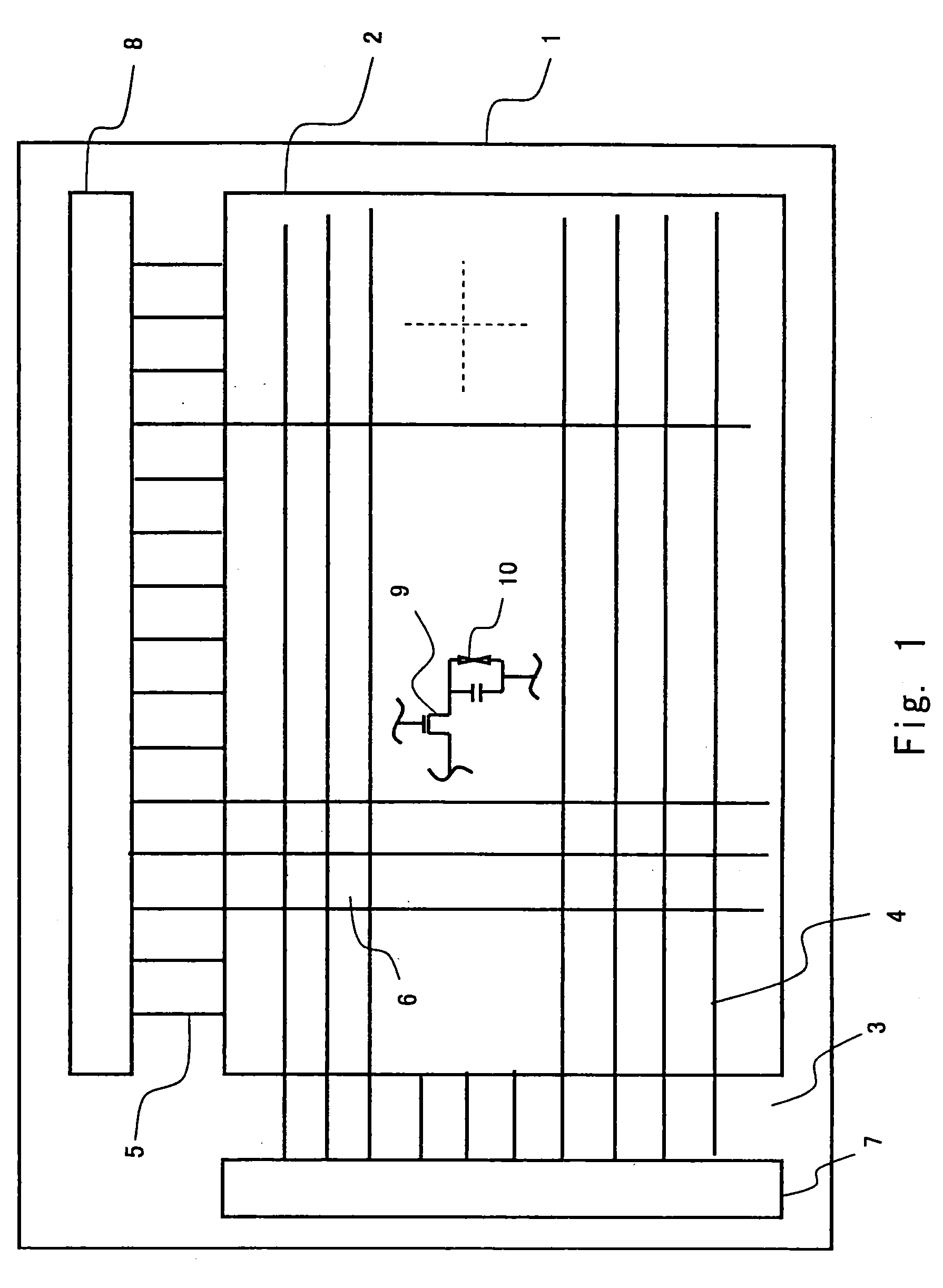
[0032]Exemplary embodiments of the present invention are described hereinafter with reference to the drawings. A thin film transistor device according to an embodiment of the present invention constitutes a TFT array substrate 1. FIG. 1 is a schematic plan view showing the structure of the TFT array substrate 1. The TFT array substrate 1 includes a display area 2 and a frame area 3 surrounding the display area 2. In the display area 2, a plurality of gate signal lines 4 and a plurality of source signal lines 5 are formed. The plurality of gate signal lines 4 are arranged in parallel with each other. Likewise, the plurality of source signal lines 5 are arranged in parallel with each other. The gate signal lines 4 and the source signal lines 5 are orthogonal to each other. Each region that is surrounded by the gate signal lines 4 and the source signal lines 5 is a pixel 6. Thus, the pixels 6 are arranged in a matrix on the TFT array substrate 1.
[0033]In the frame area 3 of the TFT arr...
second embodiment
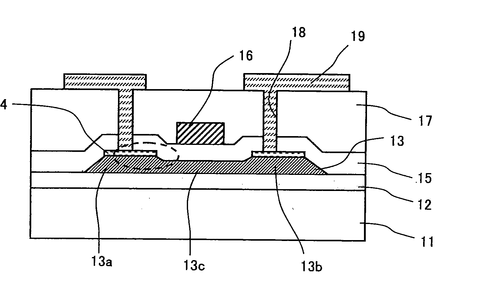
[0050]A display apparatus according to a second embodiment of the present invention is described hereinafter with reference to FIG. 7. FIG. 7 is a sectional view of the TFT device according to the second embodiment. In the TFT device of the second embodiment shown in FIG. 7, the same elements as in the first embodiment shown in FIGS. 2A to 3B are denoted by the same reference numerals and not described in detail herein.
[0051]The TFT device shown in FIG. 7 is different from the TFT device of the first embodiment shown in FIGS. 2A to 3B in that it includes an upper electrode 20 of a storage capacitor which is formed in the same layer as the gate electrode 16 and that a lamination of the metal film 14 and the polysilicon film 13 is used as a lower electrode that is opposite to the upper electrode 20 of the storage capacitor with the gate insulating film 15 interposed therebetween.
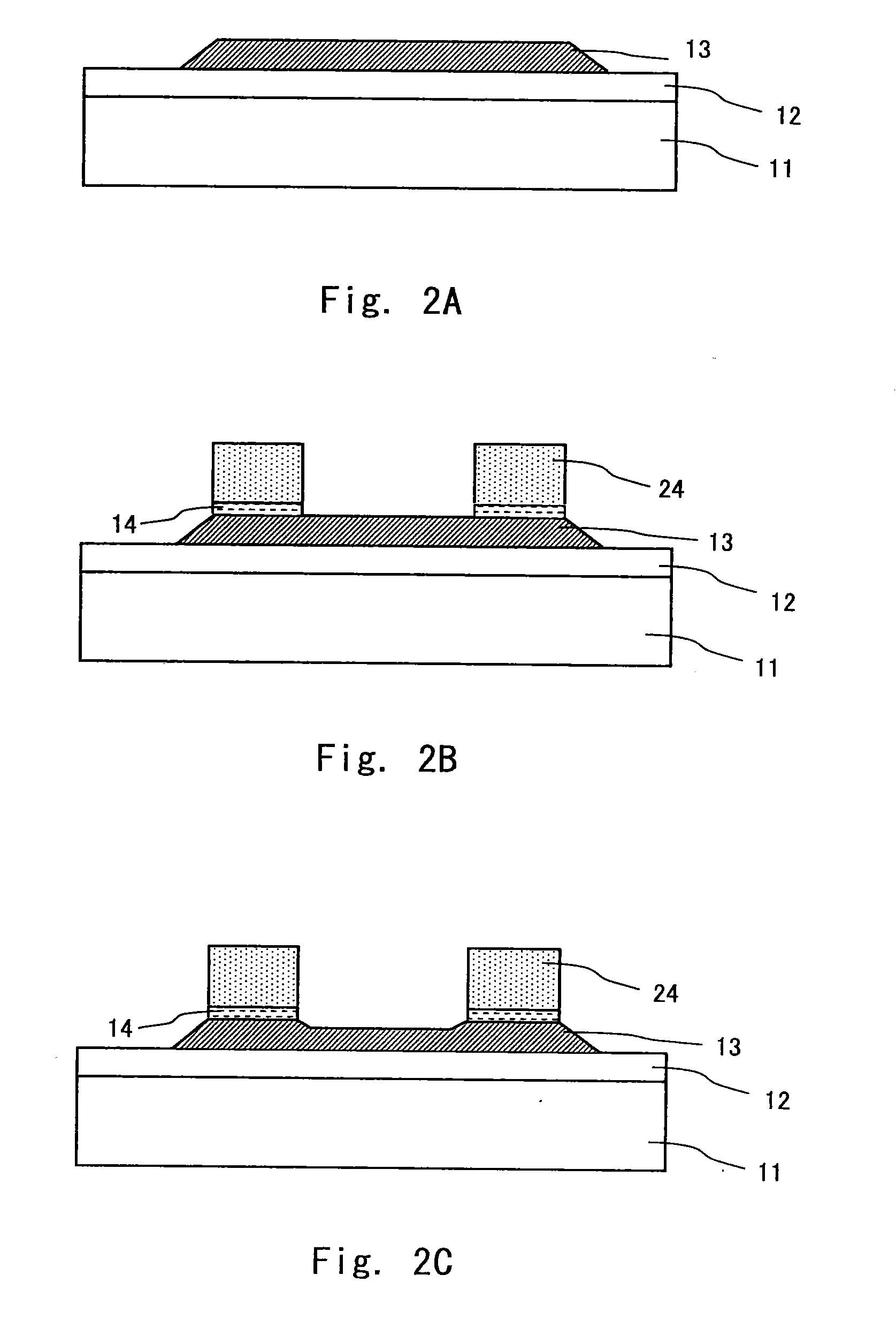
[0052]A method of manufacturing the TFT device according to this embodiment is described hereinafter in det...
third embodiment
[0057]A TFT device according to a third embodiment of the present invention is described hereinafter with reference to FIGS. 3A and 8. The TFT device shown in FIG. 8 is different from the TFT device of the first embodiment shown in FIGS. 2A to 3B in that it includes an upper insulating film 21 that is formed on the interlayer insulating film 17, a pixel electrode 23 that is formed on the upper insulating film 21, and an upper contact hole 22 to connect the pixel electrode 23 with the metal film 14.
[0058]Specifically, in the TFT device shown in FIG. 3A, the interlayer insulating film 17 and the gate insulating film 15 are etched so as to reach the metal film 14 that is formed on the source region 13a, thereby forming the contact hole 18. Then, the line electrode 19 is formed on the interlayer insulating film 17, so that it is connected with the source region 13a or the drain region 13b through the metal film 14. As the upper insulating film 21, a silicon oxide film or a silicon nitri...
PUM
 Abstract
Description
Claims
Application Information