Semiconductor device with magnetic powder mixed therein and manufacturing method thereof

a magnetic powder and semiconductor technology, applied in semiconductor devices, semiconductor/solid-state device details, electrical apparatus, etc., can solve the problems of deterioration of characteristics, inability to suppress unnecessary electromagnetic radiant noise from the upper surface, and decrease in q value of thin film induction elements, etc., to achieve the effect of suppressing unnecessary electromagnetic radiant nois

Inactive Publication Date: 2008-08-14
AOI ELECTRONICS CO LTD
View PDF11 Cites 16 Cited by
  • Summary
  • Abstract
  • Description
  • Claims
  • Application Information

AI Technical Summary

Benefits of technology

[0009]The present invention is directed to provide a semiconductor device and a manufacturing method thereof which make it possible to suppress unnecessary electromagnetic radiant noise from an integrated circuit on the upper surface side of a semiconductor substrate to the outside or from the outside to the integrated circuit on the upper surface side of the semiconductor substrate.
[0010]The present invention is also directed to reduce an eddy current loss in a thin film induction element due to an eddy current generated in a semiconductor substrate in a semiconductor device having the thin film induction element on the semiconductor substrate.
[0018]According to this semiconductor device, the insulating film and / or the sealing film is formed of a resin in which magnetic powder is mixed, so that unnecessary electromagnetic radiant noise from the integrated circuit on the upper surface side of the semiconductor substrate to the outside or from the outside to the integrated circuit on the upper surface side of the semiconductor substrate can be suppressed by the magnetic powder in the insulating film and / or the sealing film.
[0019]Furthermore, in a semiconductor device according to another aspect of this invention called a CSP comprising a spiral thin film induction element, a magnetic film in which magnetic powder is mixed in a resin is provided between a semiconductor substrate and the thin film induction element, so that it is possible to reduce an eddy current loss in the thin film induction element due to an eddy current generated in the semiconductor substrate.

Problems solved by technology

In this conventional semiconductor device, the upper surface side of the semiconductor substrate can be protected against pollution from external atmosphere and against damage owing to the sealing film made of, for example, the epoxy resin, but this semiconductor device has a problem of not being able to suppress unnecessary electromagnetic radiant noise from the upper surface side of the semiconductor substrate to the outside or from the outside to the upper surface side of the semiconductor substrate.
In this conventional semiconductor device, the spiral thin film induction element is provided on the upper surface of a protective film, so that an eddy current loss is caused in the thin film induction element by an eddy current generated in a semiconductor substrate, leading to a problem of deteriorated characteristics (a decreased Q value) of the thin film induction element.

Method used


Image

  • Semiconductor device with magnetic powder mixed therein and manufacturing method thereof
  • Semiconductor device with magnetic powder mixed therein and manufacturing method thereof
  • Semiconductor device with magnetic powder mixed therein and manufacturing method thereof

Examples


first embodiment

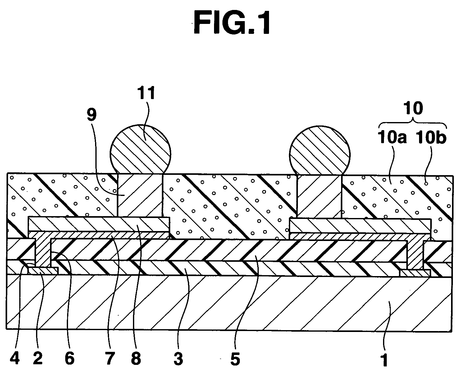
[0047]FIG. 1 is a sectional view of a semiconductor device as a first embodiment of this invention. This semiconductor device is called a CSP, and includes a silicon substrate (semiconductor substrate) 1. An integrated circuit (not shown) having a predetermined function is provided on the upper surface or one side of the silicon substrate 1, and a plurality of connection pads 2 made of a metal such as an aluminum-based metal are provided on peripheral parts of the upper surface of the silicon substrate 1 so that these connection pads are electrically connected to the integrated circuit.

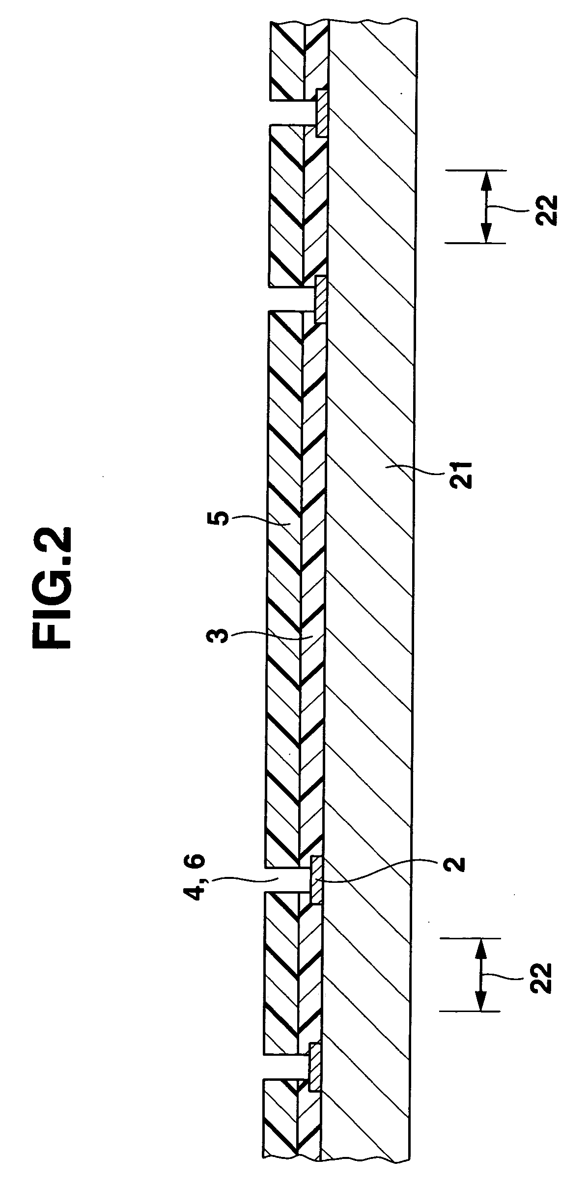
[0048]An insulating film 3 made of, for example, silicon oxide, is provided on the upper surfaces of the connection pads 2 except for the centers of the connection pads 2 and on the upper surface of the silicon substrate 1. The centers of the connection pads 2 are exposed via openings 4 formed in the insulating film 3. A protective-film 5 made of a thermosetting resin such as a polyimide resin or epox...

second embodiment

[0059]FIG. 10 is a sectional view of a semiconductor device as a second embodiment of this invention. This semiconductor device is different from the semiconductor device shown in FIG. 1 in that a protective film (insulating film) 5 is also formed of a material in which a soft magnetic powder 5b is mixed into a thermosetting resin 5a made of, for example, the polyimide resin or epoxy resin, in the same manner as a sealing film 10.

[0060]In this semiconductor device, the soft magnetic powder 10b, 5b in the sealing film 10 and the protective film 5 can further suppress unnecessary electromagnetic radiant noise from the upper surface side (integrated circuit) of a silicon substrate 1 to the outside or from the outside to the upper surface side (integrated circuit) of the silicon substrate 1 than in the case of the semiconductor device shown in FIG. 1. Moreover, in order to form the protective film 5, the material in which the soft magnetic powder 5b is mixed into the thermosetting resin...

third embodiment

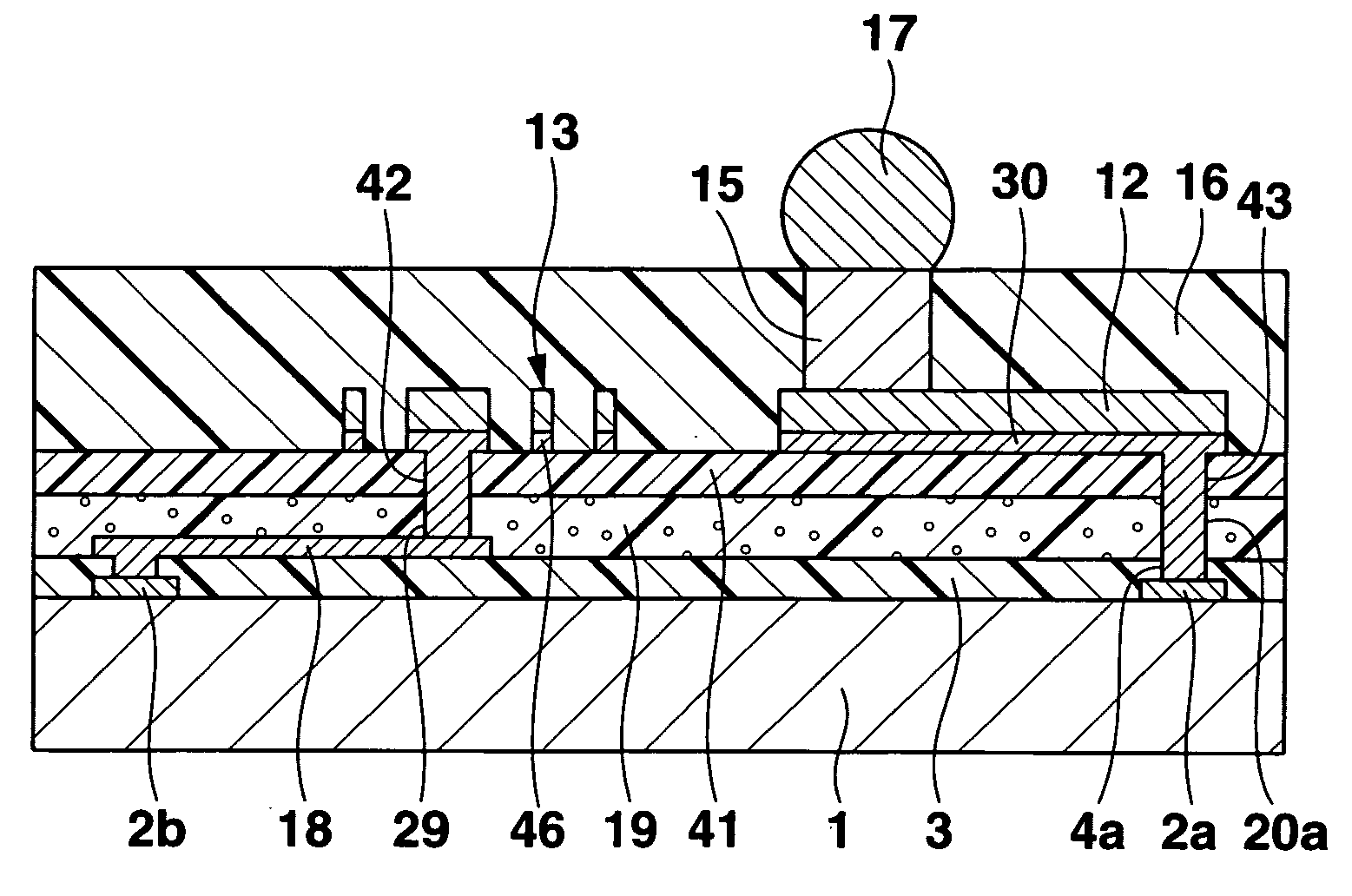
[0061]FIG. 11A is a transmitted plan view of essential parts of a semiconductor device as a third embodiment of this invention, and FIG. 11B is a sectional view along the 11B-11B line in FIG. 11A. This semiconductor device is generally called a CSP, and comprises a flat square silicon substrate (semiconductor substrate) 1. An integrated circuit (not shown) having a predetermined function is provided on the upper surface or one side of the silicon substrate 1, and a plurality of connection pads 2a, 2b, 2c made of a metal such as an aluminum-based metal are provided in peripheral parts of the upper surface of the silicon substrate 1 so that these connection pads are connected to the integrated circuit. In this case, the connection pads indicated by the numerals 2b, 2c are connected to both ends of a spiral thin film induction element 13 described later, and are arranged adjacently to each other in FIG. 11A.

[0062]An insulating film 3 made of, for example, silicon oxide, is provided on ...


PUM


Abstract

A semiconductor device includes a semiconductor substrate on one side of which an integrated circuit and a plurality of connection pads connected to the integrated circuit are provided. An insulating film is provided on the plurality of connection pads except for parts of the connection pads and on the one side of the semiconductor substrate. A plurality of wiring lines are provided to be electrically connected to the integrated circuit via the connection pads, each of the wiring lines having a connection pad portion. A plurality of columnar electrodes are respectively provided on one side of the connection pad portions of the wiring lines. A sealing film is provide on the peripheries of the columnar electrodes to cover the integrated circuit and which is provided. At least one of the insulating film and the sealing film is formed of a resin in which magnetic powder is mixed.

Description

CROSS-REFERENCE TO RELATED APPLICATIONS[0001]This application is based upon and claims the benefit of priority from prior Japanese Patent Applications No. 2007-031757, filed Feb. 13, 2007; and No. 2007-043355, filed Feb. 23, 2007, the entire contents of both which are incorporated herein by reference.BACKGROUND OF THE INVENTION[0002]1. Field of the Invention[0003]The present invention relates to a semiconductor device and a manufacturing method thereof, the semiconductor device comprising: a semiconductor substrate which includes, on one side, an integrated circuit and a plurality of connection pads connected to this integrated circuit; an insulating film provided on the one side of the semiconductor substrate except for the plurality of connection pads; a plurality of wiring lines which are provided to be electrically connected to the integrated circuit via the connection pads and which have connection pad portions; a plurality of projecting or columnar electrodes provided on one s...

Claims


Application Information

Patent Timeline
Patent Type & Authority Applications(United States)
IPC IPC(8): H01L23/485H01L21/44
CPCH01L23/3114H01L2924/01072H01L23/525H01L23/552H01L23/645H01L24/03H01L24/05H01L24/13H01L24/94H01L2224/16H01L2224/94H01L2924/01005H01L2924/01013H01L2924/01027H01L2924/01029H01L2924/0103H01L2924/01046H01L2924/01073H01L2924/01078H01L2924/14H01L2924/19015H01L23/5227H01L2224/03H01L2224/023H01L2224/0401H01L2924/0001H01L23/48
Inventor AOKI, YUTAKA
Owner AOI ELECTRONICS CO LTD
Why Eureka
Try Eureka