High voltage generation circuit and method for reducing peak current and power noise for a semiconductor memory device

a generation circuit and high voltage technology, applied in the direction of dc-dc conversion, power conversion systems, instruments, etc., can solve the problems of power noise and the peak value of consumption current to increase, and achieve the effect of reducing the peak value of consumption current and power nois

Inactive Publication Date: 2008-08-14
SAMSUNG ELECTRONICS CO LTD
View PDF10 Cites 0 Cited by
  • Summary
  • Abstract
  • Description
  • Claims
  • Application Information

AI Technical Summary

Benefits of technology

[0007]Exemplary embodiments of the present invention are directed to a high voltage generation circuit and method for reducing a peak value of consumption current and power noise by controlling a toggling period or a phase of clock signals for generating a plurality of high voltages for a semiconductor memory device. In an exemplary embodiment, the high voltage generation circuit includes a plurality of high voltage generation units configured to respectively generate high voltage signals having different voltage levels in response to first clock signals The high voltage generation units are configured to generate second clock signals based on the voltage levels of the high voltage signals, respectively. A control circuit is used to receive the second clock signals and to generate the first clock signals. The first clock signals do not toggle simultaneously based on the second clock signals.

Problems solved by technology

This causes the peak value of the consumption current and the power noise to further increase.

Method used


Image

  • High voltage generation circuit and method for reducing peak current and power noise for a semiconductor memory device
  • High voltage generation circuit and method for reducing peak current and power noise for a semiconductor memory device
  • High voltage generation circuit and method for reducing peak current and power noise for a semiconductor memory device

Examples


Embodiment Construction

[0015]The present invention will now be described more fully hereinafter with reference to the accompanying drawings, in which preferred embodiments of the invention are shown. This invention, however, may be embodied in many different forms and should not be construed as limited to the embodiments set forth herein. Rather, these embodiments are provided so that this disclosure will be thorough and complete, and will fully convey the scope of the invention to those skilled in the art. In the drawings, like numbers refer to like elements throughout. Furthermore, it will be understood that when an element is referred to as being “connected” or “coupled” to another element, it can be directly connected or coupled to the other element or intervening elements may be present. In contrast, when an element is referred to as being “directly connected” or “directly coupled” to another element, there are no intervening elements present.

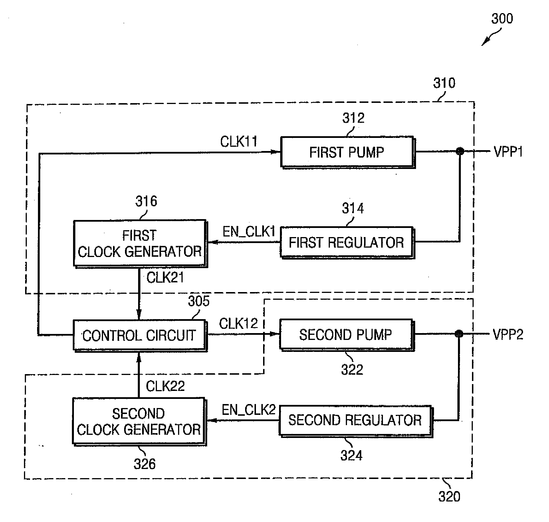
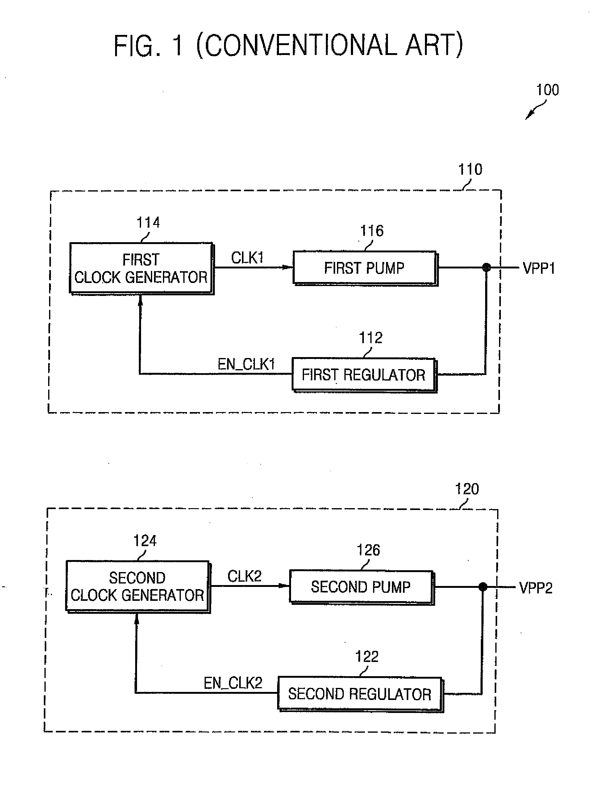
[0016]FIG. 3 is a block diagram of a high voltage generati...


PUM


Abstract

A high voltage generation circuit for use with a semiconductor memory device includes a plurality of high voltage generation units and a control circuit. The high voltage generation units generate high voltages having different voltage levels in response to corresponding clock signals. The control circuit generates clock signals, which do not toggle simultaneously, based on the voltage levels of the high voltages.

Description

CROSS-REFERENCE TO RELATED APPLICATION[0001]This U.S. non-provisional application claims priority under 35 U.S.C. § 119 of Korean Patent Application No. 10-2007-0014467 filed on Feb. 12, 2007 the entire contents of which are hereby incorporated by reference.BACKGROUND OF THE INVENTION[0002]1. Field of the Invention[0003]Embodiments of the invention relate to a high voltage generation circuit for a semiconductor memory device. More particularly, embodiments of the invention relate to a high voltage generation circuit and method for reducing a peak value of consumption current and power noise.[0004]2. Description of the Related Art[0005]Semiconductor memory devices such as NAND flash memories, NOR flash memories, and electrically erasable programmable read-only memories (EEPROM) use a voltage higher than a normal power supply voltage to program or erase memory cells. For example, a flash memory device needs voltages having different voltage levels when performing program, erase, and r...

Claims


Application Information

Patent Timeline
Patent Type & Authority Applications(United States)
IPC IPC(8): G05F3/02
CPCG11C16/30G11C5/145G11C5/14G11C16/32
Inventor KWON, OH SUKCHOI, KI HWAN
Owner SAMSUNG ELECTRONICS CO LTD
Why Eureka
Try Eureka