
Protection device for a semiconductor switch, and method for operating a protection device for a semiconductor switch

a protection device and semiconductor technology, applied in the direction of electronic switching, electrical equipment, pulse technique, etc., can solve the problems of said semiconductor switch being thermally destroyed, said semiconductor switch being damaged, etc., to achieve the effect of rapid protection of the semiconductor switch, quick transfer into a conductive state, and more rapid respons

Active Publication Date: 2016-01-07
ROBERT BOSCH GMBH
View PDF3 Cites 1 Cited by
  • Summary
  • Abstract
  • Description
  • Claims
  • Application Information

AI Technical Summary

Benefits of technology

The present invention is about a surge protection system for a semiconductor switch. The system has a two-stage process. Initially, when the voltage at the switch reaches a certain threshold, it is only briefly activated to prevent the switch from becoming constantly conductive. This temporary activation allows the surge protection to respond quickly and ensures effective protection of the switch. In a second stage, once the voltage exceeds a higher threshold, the switch is permanently activated, resulting in a quicker response time and lower peak values of transient surge pulses. The switch detector is designed to keep the surge protection system inactive when the switch is closed or off to prevent external triggers.

Problems solved by technology

If the resulting voltage exceeds the maximum reverse voltage of the semiconductor switch, said semiconductor switch can then be destroyed.
Otherwise the danger exists that the semiconductor switch passes over into a continuous operation which would lead to the thermal destruction of said semiconductor switch.

Method used


Image

  • Protection device for a semiconductor switch, and method for operating a protection device for a semiconductor switch
  • Protection device for a semiconductor switch, and method for operating a protection device for a semiconductor switch
  • Protection device for a semiconductor switch, and method for operating a protection device for a semiconductor switch

Examples


Embodiment Construction

[0023]Semiconductor switches in accordance with the present invention include all types of switching elements with which an electrical connection can be closed or opened on the basis of a semiconductor structure. The opening and closing of the semiconductor takes place by actuating the semiconductor switch by means of an electrical signal. Semiconductor switches in accordance with the present invention are in particular MOSFETs or IGBTs (Insulated gate bipolar transistors). In addition, the inventive protection device can likewise be used with all other types of semiconductor switches.

[0024]Even though the present protection device has been described in connection with semiconductor switches, said device can be used with all other switching elements with which a protection against voltage surges is to be achieved by closing the switching element.

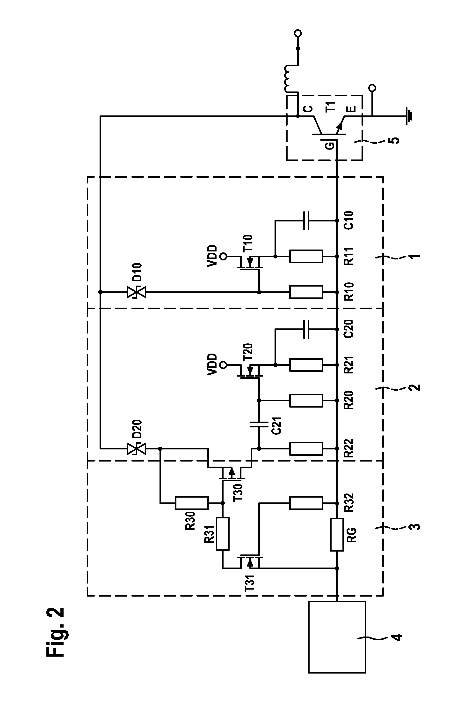
[0025]FIG. 2 shows a schematic depiction of a circuit diagram of a switching device for a semiconductor switch according to one embodiment ...


PUM


Abstract

The invention relates to a surge protection device for a semiconductor switch with an improved response behavior. The protection device comprises a dynamic component together with a static component and a capability to analyze switch operations on the semiconductor switch. The dynamic component of the surge protection device activates in the event of a low surge, but is time-limited, however, with respect to the response behavior. Furthermore, the response of the dynamic component of the surge protection device can also be limited such that a response occurs only after switch operations on the semiconductor switch.

Description

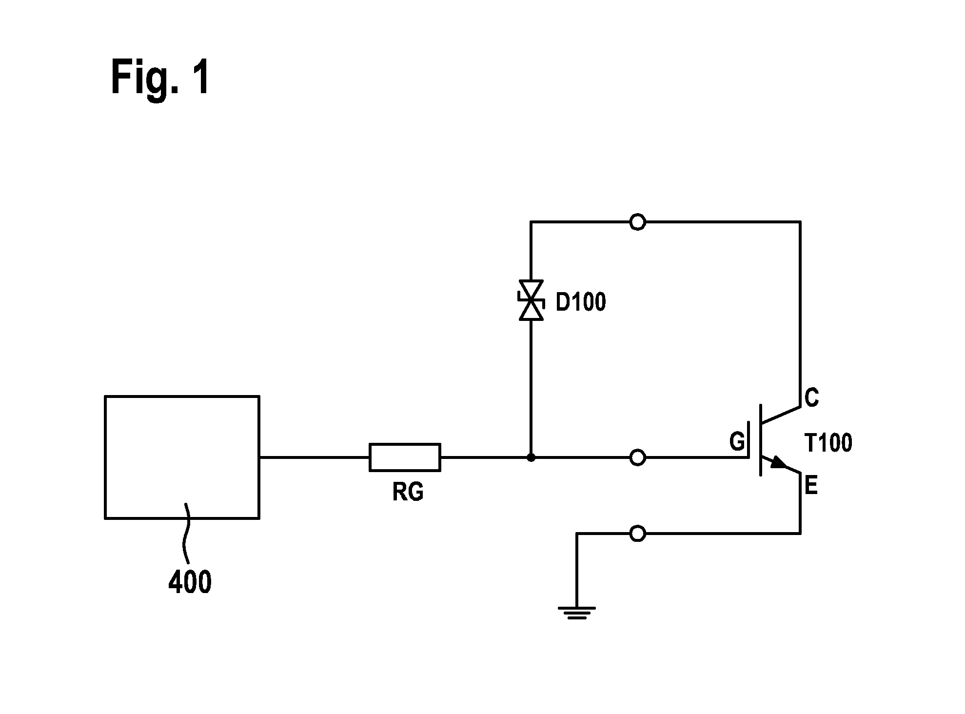
BACKGROUND OF THE INVENTION[0001]The present invention relates to a protection device for a semiconductor switch for protection against voltage surges as well as to a method for operating a protection device for a semiconductor switch in order to protect against voltage surges.[0002]The use of semiconductor switches as electrical switching elements is known. Hence, voltage surges occur upon opening the switching elements, in particular in power electronic systems, such as, for example, in DC-DC converters or in inverters, on account of the always present leakage inductances. If the current flow through a semiconductor switch is interrupted, the voltage at the semiconductor switch between collector and emitter then increases to a value which can be greater than the supply voltage. If the resulting voltage exceeds the maximum reverse voltage of the semiconductor switch, said semiconductor switch can then be destroyed.[0003]FIG. 1 shows a simple protection circuit for protecting a semi...

Claims


Application Information

Patent Timeline
Patent Type & Authority Applications(United States)
IPC IPC(8): H03K17/082
CPCH03K17/0828
Inventor LAICH, SEBASTIANSINN, PETER
Owner ROBERT BOSCH GMBH
Learn More