Method for determining lithographic focus and exposure
a technology of focus and exposure, applied in the field of photolithography methods and systems, can solve the problems of short circuits, reducing the selling price of chips, and final circuits that cannot be properly run or run at all
- Summary
- Abstract
- Description
- Claims
- Application Information
AI Technical Summary
Benefits of technology
Problems solved by technology
Method used
Image

Examples
Embodiment Construction
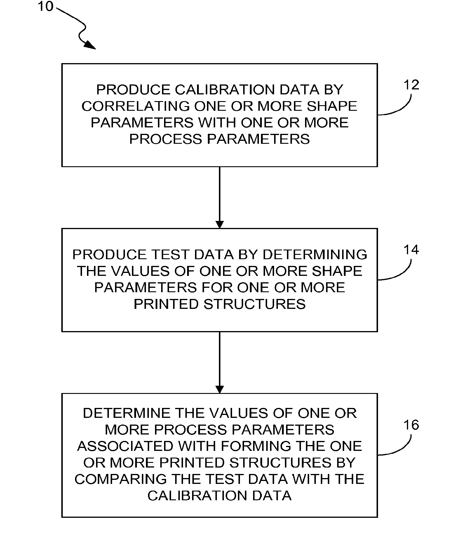
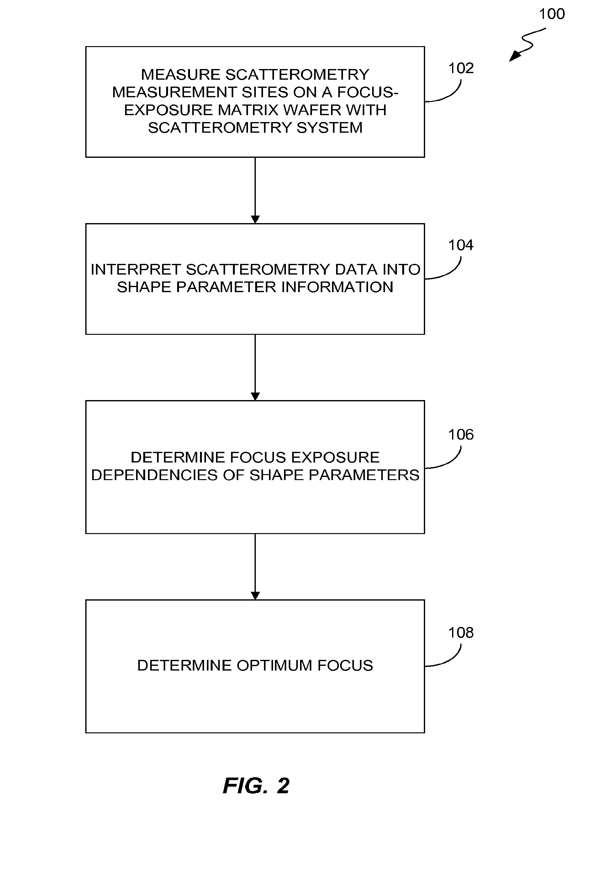
[0034]The invention generally pertains a method for determining focus and / or exposure settings of a photolithographic system (e.g., stepper or scanner). One aspect of the invention relates to determining focus and / or exposure simultaneously. Another aspect of the invention relates to using more than one shape parameter to solve for focus and exposure. Another aspect of the invention relates to using shape information derived from scatterometry to determine best focus and / or exposure. This is generally accomplished by measuring and analyzing focus-exposure matrix wafer (or wafers). In some cases, a single target type is used, and in other cases, multiple target types are used. Another aspect of the invention relates to using shape information derived from scatterometry to determine the stepper or scanner focus and / or exposure on nominally processed wafers. In some cases, this is accomplished with a single target type, and in other cases, this is accomplished with multiple target type...
PUM
| Property | Measurement | Unit |
|---|---|---|
| wavelengths | aaaaa | aaaaa |
| wavelengths | aaaaa | aaaaa |
| width | aaaaa | aaaaa |
Abstract
Description
Claims
Application Information