Illumination System for a Microlithgraphic Exposure Apparatus
an exposure apparatus and illumination system technology, applied in the field of illumination systems for microlithographic projection exposure apparatuses, can solve the problems of difficult to meet tight specifications in illumination systems
- Summary
- Abstract
- Description
- Claims
- Application Information
AI Technical Summary
Benefits of technology
Problems solved by technology
Method used
Image
Examples
first embodiment
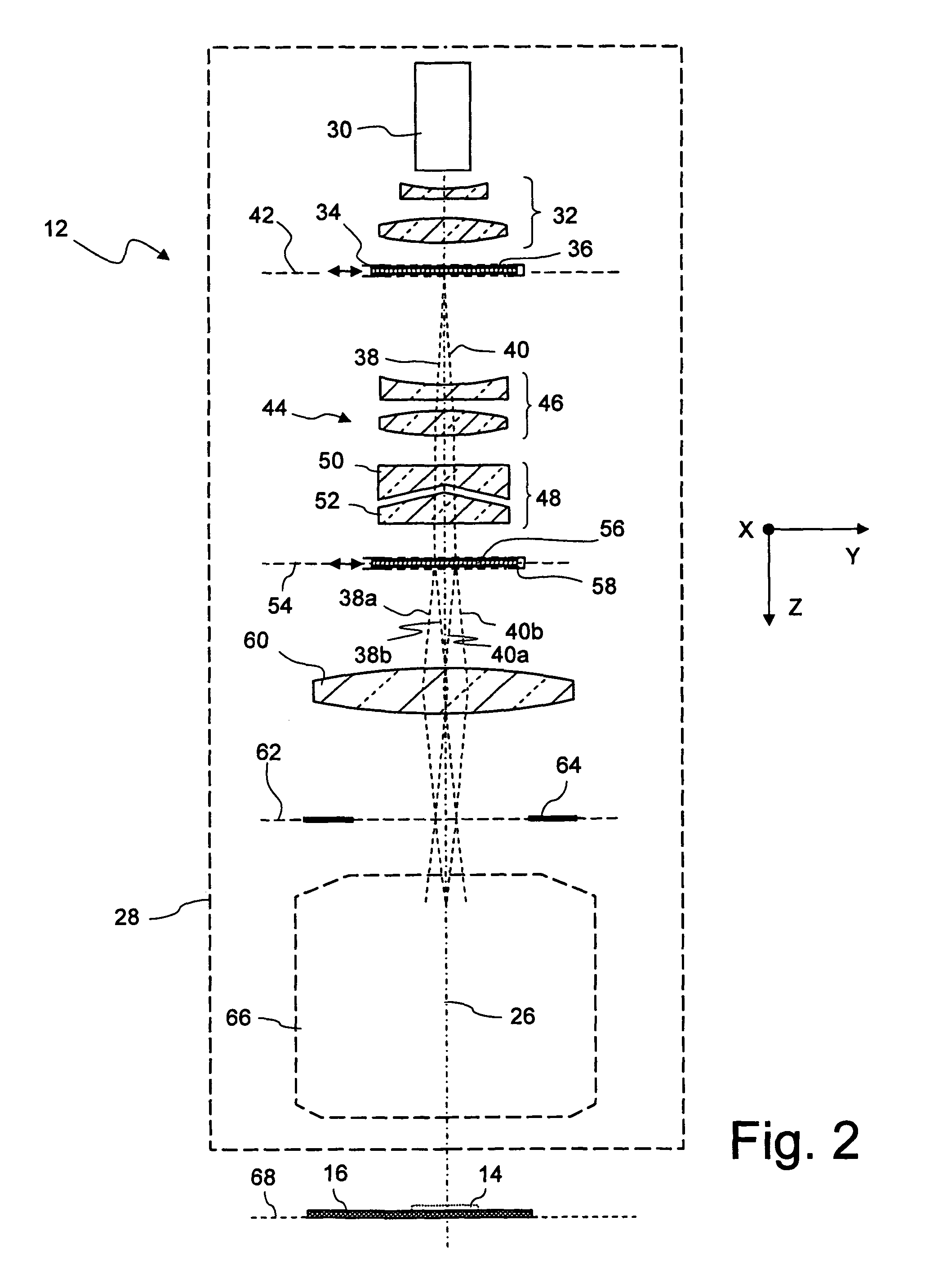
[0049]FIG. 3 shows a meridional section of the condenser 60 that is denoted in its entirety by 601. An aperture stop AS arranged in the pupil plane 54 may be formed by the rim of the second optical raster element 56. The pupil of the condenser 601 has a diameter of about 125 mm. The condenser 601 fourier-transforms the pupil to a field having a diameter of about 110 mm. The overall focal length of the condenser 601 is about 208 mm, and the image side numerical aperture is about 0.3. These values also apply to the other embodiments described further below.
[0050]Immediately behind the pupil plane 54 a first lens formed as a thin planar plate L11 made of quartz glass is positioned. The thin plate L11 as such does not substantially contribute to the optical properties of the condenser 601. However, it may support various functional elements such as a grey filter, a diffusing surface or a structure designed to selectively modify the state of polarization 15 of traversing light rays. Depe...
second embodiment
[0073]FIG. 4 shows a condenser 60 which is denoted in its entirety by 602. The lens data and the aspherical constants are given in Table 4 and 5, respectively.
TABLE 4Lens data of embodiment #2MATE-½S#RADIUSTHICKNESSRIALDiametern(193.38)1∞25.000062.541.0000002∞4.0000CAF269.401.5014843∞2.500070.121.000000 4*172.0745612.3100CAF274.951.5014845222.75300103.781075.531.0000006−117.1646035.0000SI0289.651.5602937−118.847301.1540101.021.00000087987.0000062.2400SI02109.901.560293 9*−161.383410.5000112.211.00000010 126.3670041.4500SI0293.521.56029311 298.5540035.304087.001.00000012 −276.6740011.0000SI0280.511.56029313*111.6429537.314971.131.00000014 ∞26.6900SI0270.801.56029315 −168.1372016.756570.661.00000016 ∞3.0500SI0260.451.56029317 ∞16.950059.851.000000
TABLE 5Aspherical constants of embodiment #2S#kABCD40.84843E+00−0.57629E−07−0.41326E−11−0.41876E−15−0.21243E−209−0.74026E+000.41420E−07−0.18061E−110.66307E−16−0.22252E−2013−0.99518E+00−0.12832E−060.23043E−10−0.22350E−140.81039E−19
[0074]The co...
third embodiment
[0080]FIG. 5 shows a meridional section through a condenser 603 according to a The lens data and the aspherical constants are given in Tables 6 and 7, respectively.
[0081]The condenser 603 is, both in terms of optical design and optical properties (cf. Table 3), comparable to the condenser 602. However, the lenses L23 and L24 are combined to form a single thick meniscus lens L33. Only the plate L31 and the first thin meniscus lens L32 are made of CaF2 or a similar material. All other optical elements of the condenser 603 may be made of a conventional lens material such as quartz glass.
TABLE 6Lens data of embodiment #3MATE-½S#RADIUSTHICKNESSRIALDiametern(193.38)1∞25.000064.861.0000002∞4.0000CAF271.721.5014843∞2.500072.431.000000 4*200.0411014.5000CAF277.081.5014845233.03400124.685877.771.0000006−389.1060060.0000SI02104.661.560293 7*−114.203520.5000110.581.000000 8*128.2895962.8300SI02101.091.56029391000.1700011.090292.721.00000010 −1778.9600010.0000SI0290.561.56029311*83.5000043.1940...
PUM
 Abstract
Description
Claims
Application Information


